 | –≠–ª–µ–∫—Ç—Ä–æ–Ω–Ω—ã–π –∫–æ–º–ø–æ–Ω–µ–Ω—Ç: S-80717AL | –°–∫–∞—á–∞—Ç—å:  PDF PDF  ZIP ZIP |

Contents
Features........................................................... 1
Applications ..................................................... 1
Pin Assignment................................................ 1
Block Diagram ................................................. 2
Selection Guide ............................................... 3
Output Configurations...................................... 4
Advantage over the S-805 Series.................... 5
Absolute Maximum Ratings............................. 6
Electrical Characteristics ................................. 7
Test Circuits................................................... 23
Technical Terms ............................................ 24
Operation ....................................................... 26
Dimensions .................................................... 28
Taping............................................................ 29
Magazine Dimensions ................................... 31
Markings ........................................................ 32
Characteristics ............................................... 33
Measuring Circuits ......................................... 36
Application Circuit Examples ......................... 37
Notes ............................................................. 39
Frequently Asked Questions......................... 40
Seiko Instruments Inc.
1
*
S-807 Series will be summarized into S-808 Series.
HIGH-PRECISION VOLTAGE DETECTOR
S-807 Series
The S-807 Series is an adjustment-free high-precision voltage detector
made using the CMOS process. The output voltage is fixed internally,
with an accuracy of
±
2.4%. Two output types are available, Nch open-
drain and CMOS output (active "H" and "L"), both of which have various
product lineups. This series features much lower current consumption
and higher detection voltage accuracy than the S-805 Series. Super-
miniature package is added for the S-807 Series, the S-807XXSX
Series. This small SOT-23-5 style package allows the designer to
shrink the size of his finished product. Electrical specs for the S-
807XXSX Series are the same as the standard S-807 Series. Output
forms of the S-807XXSX Series are Nch open-drain and CMOS active
"L".
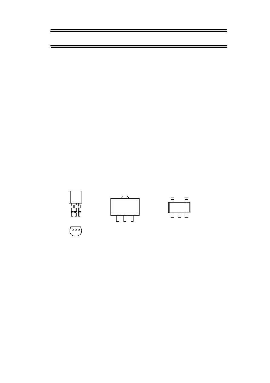
Pin Assignment
Features
∑
Ultra-low current consumption
1.0
µ
A typ. (V
DD
=4.5 V)
∑
High-precision detection voltage
±
2.4%
∑
Wide operating voltage range
1.0 to 15 V
∑
Good hysteresis characteristics
5% typ.
∑
Wide operating temperature range
-30
∞
C to+80
∞
C
∑
3 output forms : Nch open-drain, CMOS output active H ,
active L
∑
TO-92, SOT-89-3 and SOT-23-5 package
Applications
∑
Battery checker
∑
Battery backup for memories
∑
Power failure detector
∑
Reset for microcomputer
∑
Store signal detector for non-
volatile RAM
Top view
Top view
1 OUT
2 V
DD
3 V
SS
1 2 3
Bottom view
1
2
3
1 OUT
2 V
DD
3 V
SS
(1) TO-92
(2) SOT-89-3
(3) SOT-23-5
1
2
3
1 OUT
2 V
DD
3 V
SS
4
NC
5
NC
5
4
Figure 1
HIGH-PRECISION VOLTAGE DETECTOR
S-807 Series
2
Seiko Instruments Inc.
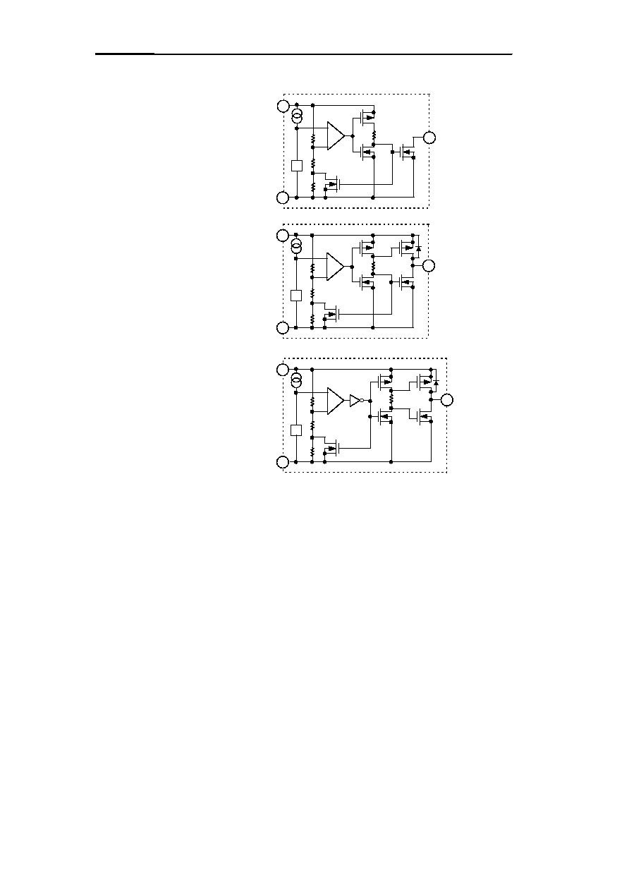
Block Diagram
+
-
OUT
V
DD
2
V
SS
3
1
(1) Nch open-drain output
(2) CMOS active low output
(3) CMOS active high output
Figure 2
-
+
OUT
V
SS
V
DD
2
3
1
-
+
OUT
V
SS
V
DD
2
3
1
*
*
* Parasitic diode
HIGH-PRECISION VOLTAGE DETECTOR
S-807 Series
Seiko Instruments Inc.
3
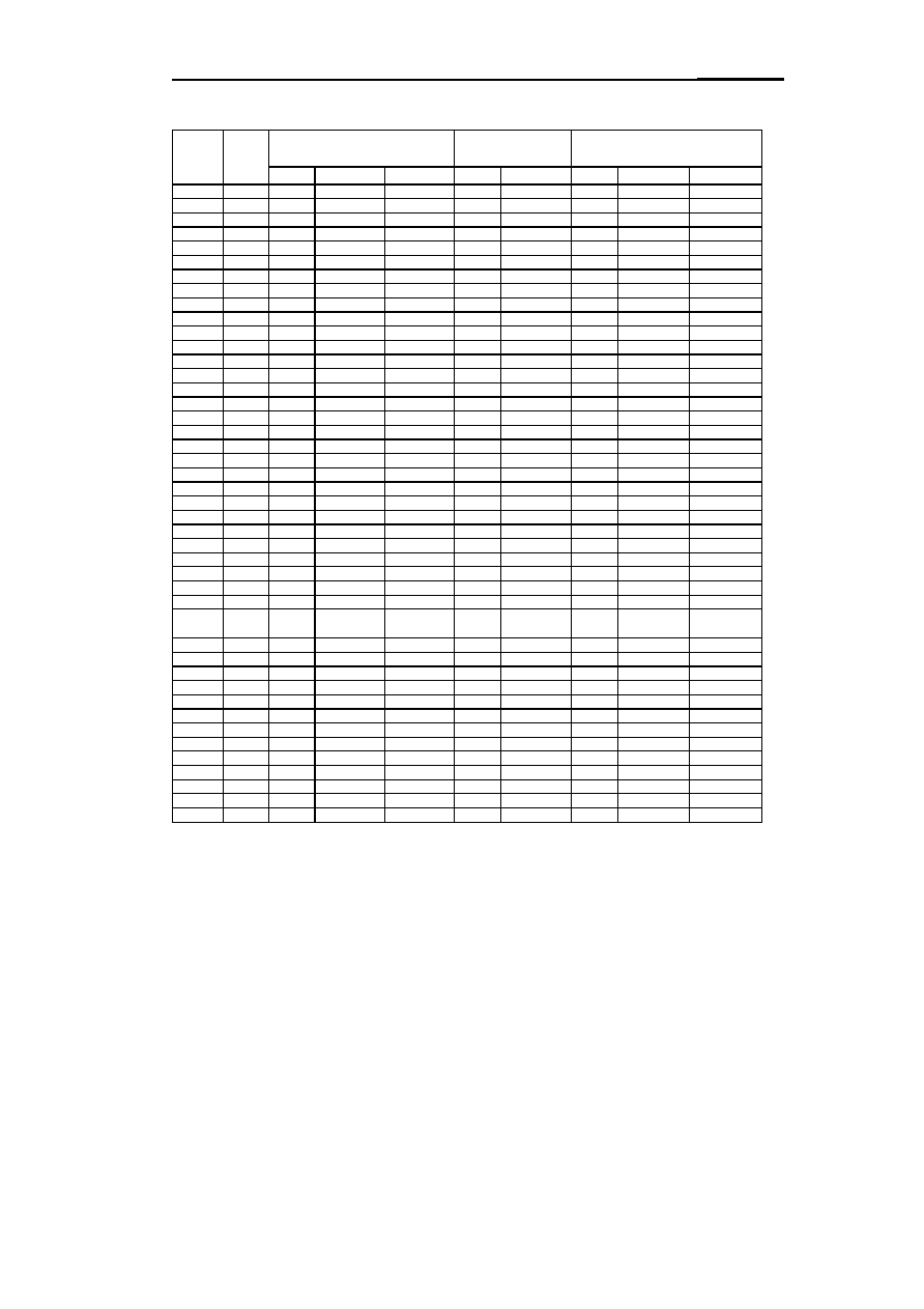
Selection Guide
Table 1
Detection
voltage
range (V)
Hysteresis
width
typ. (V)
CMOS output (Low)
CMOS output (High)
Nch open-drain
TO-92
SOT-89-3*
SOT-23-5*
TO-92
SOT-89-3*
TO-92
SOT-89-3*
SOT-23-5*
1.5 V
±
2.4%
0.075
S-80715AL-AC-X
S-80715AN-DC-X
1.6 V
±
2.4%
0.08
S-80716AL-AD-X
S-80716AN S-80716AN-DD-X
1.7 V
±
2.4%
0.085
S-80717AL S-80717AL-AE-X
S-80717AN S-80717AN-DE-X S-80717SN-DE-X
1.8 V
±
2.4%
0.09
S-80718AL S-80718AL-AF-X S-80718SL-AF-X
S-80718AH-BF-T1 S-80718AN S-80718AN-DF-X
1.9 V
±
2.4%
0.095
S-80719AL S-80719AL-AG-X S-80719SL-AG-X
S-80719AN S-80719AN-DG-X S-80719SN-DG-X
2.0 V
±
2.4%
0.1
S-80720AL-AH-X S-80720SL-AH-X
S-80720AN S-80720AN-DH-X S-80720SN-DH-X
2.1 V
±
2.4%
0.105
S-80721AL S-80721AL-AJ-X
S-80721SL-AJ-X
S-80721AN S-80721AN-DJ-X
S-80721SN-DJ-X
2.2 V
±
2.4%
0.11
S-80722AL S-80722AL-AK-X
S-80722AN S-80722AN-DK-X
2.3 V
±
2.4%
0.115
S-80723AL S-80723AL-AL-X
S-80723SL-AL-X
S-80723AN S-80723AN-DL-X
S-80723SN-DL-X
2.4 V
±
2.4%
0.12
S-80724AL S-80724AL-AM-X
S-80724AN S-80724AN-DM-X S-80724SN-DM-X
2.5 V
±
2.4%
0.125
S-80725AL S-80725AL-AN-X S-80725SL-AN-X
S-80725AH-BN-X S-80725AN S-80725AN-DN-X S-80725SN-DN-X
2.6 V
±
2.4%
0.13
S-80726AL-AP-X
S-80726AN S-80726AN-DP-X
2.7 V
±
2.4%
0.135
S-80727AL S-80727AL-AQ-X S-80727SL-AQ-X
S-80727AN S-80727AN-DQ-X S-80727SN-DQ-X
2.8 V
±
2.4%
0.14
S-80728AL-AR-X S-80728SL-AR-X
S-80728AN S-80728AN-DR-X S-80728SN-DR-X
2.9 V
±
2.4%
0.145
S-80729AL S-80729AL-AS-X
S-80729AN-DS-X
3.0 V
±
2.4%
0.15
S-80730AL S-80730AL-AT-X S-80730SL-AT-X
S-80730AN S-80730AN-DT-X S-80730SN-DT-X
3.1 V
±
2.4%
0.155
S-80731AL S-80731AL-AV-X
S-80731AH S-80731AH-BV-X S-80731AN S-80731AN-DV-X
3.2 V
±
2.4%
0.16
S-80732AL S-80732AL-AW-X S-80732SL-AW-X
S-80732AN S-80732AN-DW-X
3.3 V
±
2.4%
0.165
S-80733AL S-80733AL-AX-X S-80733SL-AX-X S-80733AH
S-80733AN S-80733AN-DX-X S-80733SN-DX-X
3.4 V
±
2.4%
0.17
S-80734AL S-80734AL-AY-X
S-80734AN S-80734AN-DY-X
3.5 V
±
2.4%
0.175
S-80735AL S-80735AL-AZ-X S-80735SL-AZ-X
S-80735AN S-80735AN-DZ-X S-80735SN-DZ-X
3.6V
±
2.4%
0.18
S-80736AL-A0-X
S-80736AN S-80736AN-D0-X
3.7V
±
2.4%
0.185
S-80737AL S-80737AL-A1-X
S-80737AN S-80737AN-D1-X
3.8 V
±
2.4%
0.19
S-80738AL S-80738AL-A2-X
S-80738AN S-80738AN-D2-X
3.9 V
±
2.4%
0.195
S-80739AL S-80739AL-A3-X
S-80739AN S-80739AN-D3-X
4.0 V
±
2.4%
0.2
S-80740AL S-80740AL-A4-X
S-80740SL-A4-X S-80740AH S-80740AH-B4-X S-80740AN S-80740AN-D4-X
S-80740SN-D4-X
4.1 V
±
2.4%
0.205
S-80741AL S-80741AL-A5-X
S-80741AN S-80741AN-D5-X
4.2 V
±
2.4%
0.21
S-80742AL S-80742AL-A6-X
S-80742SL-A6-X
S-80742AN S-80742AN-D6-X
S-80742SN-D6-X
4.3 V
±
2.4%
0.215
S-80743AL S-80743AL-A7-X
S-80743AN S-80743AN-D7-X
4.4 V
±
2.4%
0.22
S-80744AL S-80744AL-A8-X
S-80744AN S-80744AN-D8-X
S-80744SN-D8-X
4.295
to
4.605
Release
voltage
4.70 max.
S-80744HL S-80744HL-U8-X
4.5 V
±
2.4%
0.225
S-80745AL S-80745AL-A9-X
S-80745SL-A9-X
S-80745AH-B9-X S-80745AN S-80745AN-D9-X
S-80745SN-D9-X
4.6 V
±
2.4%
0.23
S-80746AL S-80746AL-EA-X
S-80746AN-JA-X
4.7 V
±
2.4%
0.235
S-80747AL S-80747AL-EB-X
S-80747AN-JB-X
4.8 V
±
2.4%
0.24
S-80748AL-EC-X
S-80748AN S-80748AN-JC-X
4.9 V
±
2.4%
0.245
S-80749AL-ED-X
S-80749AN-JD-X
5.0 V
±
2.4%
0.25
S-80750AL-EE-X S-80750SL-EE-X
S-80750AN S-80750AN-JE-X
S-80750SN-JE-X
5.1 V
±
2.4%
0.255
S-80751AL
S-80751SL-EF-X
S-80751AN S-80751AN-JF-X
S-80751SN-JF-X
5.2 V
±
2.4%
0.26
S-80752AL-EG-T1 S-80752SL-EG-T1
S-80752AN-JG-T1
5.3 V
±
2.4%
0.265
S-80753AN
5.5 V
±
2.4%
0.275
S-80755AL-EK-X
6.1 V
±
2.4%
0.305
S-80761SL-ER-X
6.3 V
±
2.4%
0.315
S-80763AN-JT-X
7.7V
±
2.4%
0.385
S-80777SN-J8-X
*
The last digit of the model name changes depending upon the packing form when it is an SOT package product (S-807XXSX
Series is packed on tape).
S : Stick
T : Tape (T1 and T2 types are available depending on the direction of detectors on the tape.)
** Please ask our sales person if you need another detection voltage product.
HIGH-PRECISION VOLTAGE DETECTOR
S-807 Series
4
Seiko Instruments Inc.
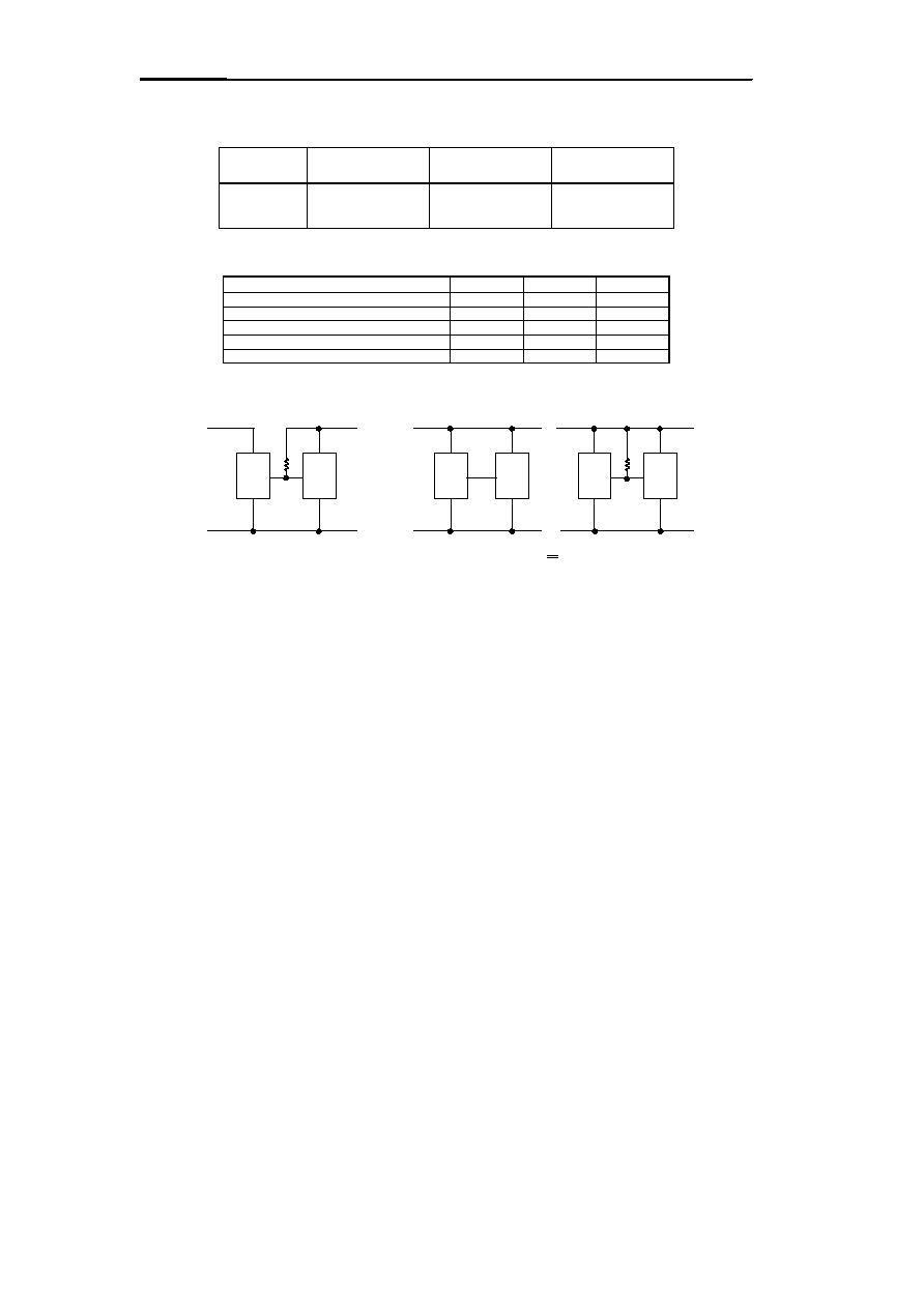
Output Configurations
1. S-807 Series model numbering conventions
Nch open-drain
(
"
L
"
reset type)
CMOS output
(
"
L
"
reset type)
CMOS output
(
"
H
"
reset type)
S-807 Series
"
N
"
is the last letter of
the model number.
Ex. S-80732AN
"
L
"
is the last letter of
the model number.
Ex. S-80718AL
"
H
"
is the last letter of
the model number.
Ex. S-80740AH
2. Output configurations and their implementations
Implementation
Nch
CMOS (
"
L
"
)
CMOS (
"
H
"
)
With different power supplies
◊
◊
With active low reset CPUs
◊
With active high reset CPUs
◊
◊
As power resets employing CR circuits
◊
◊
With voltage divider resistors to vary (-V
DET
)
◊
◊
V / D
CMOS
V
DD
V
SS
OUT
V
DD
2
V
DD
1
V / D
Nch
CPU
∑
Example with two power supplies
V
SS
OUT
CPU
V
SS
V
DD
V / D
Nch
CPU
∑
Examples with one power supply
or
Figure 3
OUT
HIGH-PRECISION VOLTAGE DETECTOR
S-807 Series
Seiko Instruments Inc.
5
Advantage over the S-805 Series
The S-807 Series, in comparison with conventional reset ICs such as the S-805 Series, offers greater detection voltage precision
(twice that of conventional units) and lower current consumption (half that of conventional units). These characteristics result in
the following advantages over conventional units.
1. Advantages of greater detection voltage precision
1.1 Detecting lithium battery service life
The discharge characteristics of lithium batteries are
shown in Figure 4. When using the S-805 Series,
the service life can be detected over t1. When
using the S-807 Series, it can be detected over t2.
This improvement in detection precision of the S-
807 Series means that batteries can be used over
more of their service life.
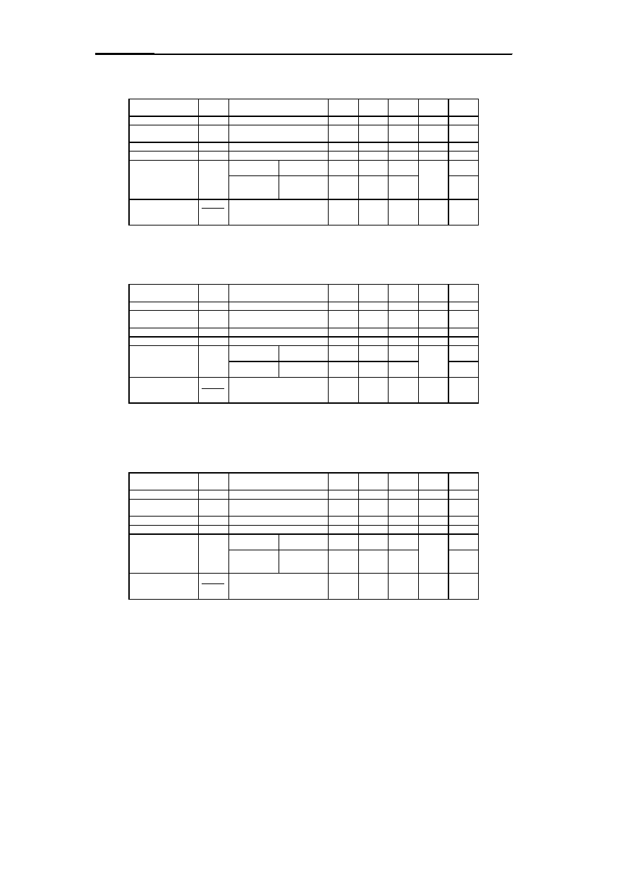
1.2 Detecting a power voltage at two points
It is usual for the CPU to detect the power voltage
at two points, one to caution and the other to reset.
The service life of battery may also be detected at
two points, one to caution and the other to request
immediate replacement.
Two voltage values to be detected (No. 1 and No.
2) do not cross and the voltage can be detected
correctly.
1.3 Voltage drop when modifying detection voltage
If no voltage to be detected is suitable, the voltage
can be set higher in Nch open-drain output
products by using a resistor divider. (Example :
when detecting 6V or 9V.)
When 8V is detected using the S-8054HN (a
4V
±
5% device), the -Vdet tolerance becomes
2
◊
4.00
ױ
0.05=0.8V (R1=R2). In constrast, the S-
80740AN (a 4V
±
2.4% device) can hold down the
tolerance to 2
◊
4.00
ױ
0.024=0.384V (R1=R2).
Must be close
V
t
No. 2
No. 1
Figure 5
t1
S-807
S-805
V
t
Figure 4
t2
R2
R1
Figure 6
Nch open-drain
output product
S-807
XXAN/SN
HIGH-PRECISION VOLTAGE DETECTOR
S-807 Series
6
Seiko Instruments Inc.
2. Others
2.1 Low current consumption
The current consumption is half of that of a conventional voltage detection IC, so the battery service life can be
prolonged.
2.2 Wide operating voltage range
The maximum operating voltage of a conventional IC is 10 V. For the S-807 Series, the maximum detectable voltage
has been increased to 15 V.
Absolute Maximum Ratings
Parameter
Symbol
Ratings
Unit
Power supply voltage
V
DD
-V
SS
18
V
Input voltage
V
IN
V
SS
-0.3 to V
DD
+0.3
Output
voltage
Nch
open-drain
V
OUT
V
SS
-0.3 to 18
CMOS
V
SS
-0.3 to V
IN
+0.3
Output current
I
OUT
50
mA
Power dissipation
P
D
TO-92, SOT-89-3
200
mW
SOT-23-5
150
Operating temperature
T
opr
-30 to +80
∞
C
Storage temperature
T
stg
-40 to +125
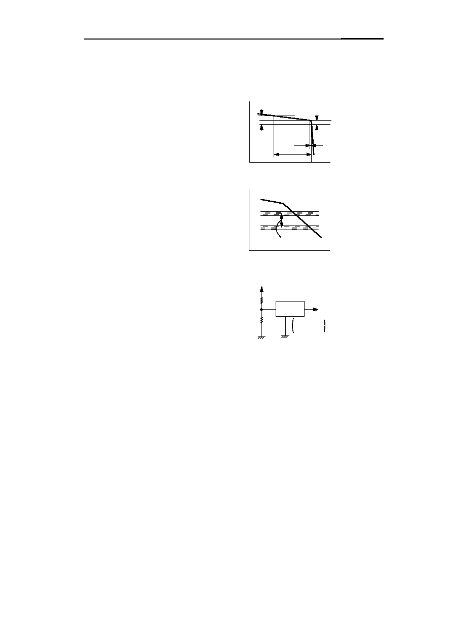
1.4 Operating margins of power and minimum operating voltage
of CPU are close
Set the voltage so that it will be detected between the power
voltage and the minimum operating voltage of the CPU.
Thus, if two voltage points to be detected are very close, the
voltage between those two points must be detected
correctly. The S-807 Series offers an excellent detection
voltage precision, so the voltage between narrow limits can
be detected correctly.
V
t
5 V
Min. operating
voltage of CPU
Reset voltage to be detected
Figure 7
(Unless otherwise specified : Ta=25
∞
C)
Caution : Keep static electricity to a minimum
.
HIGH-PRECISION VOLTAGE DETECTOR
S-807 Series
Seiko Instruments Inc.
7
Electrical Characteristics
1.
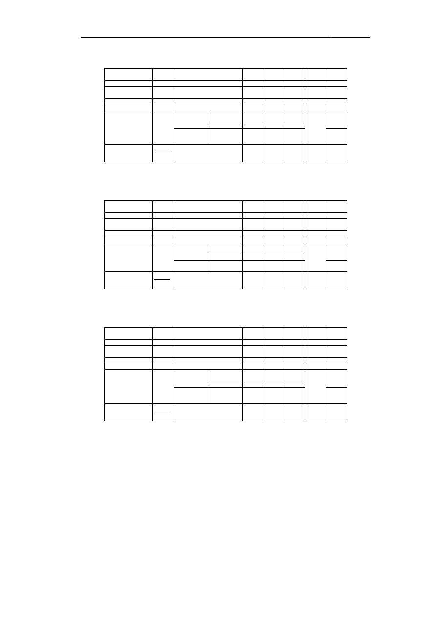
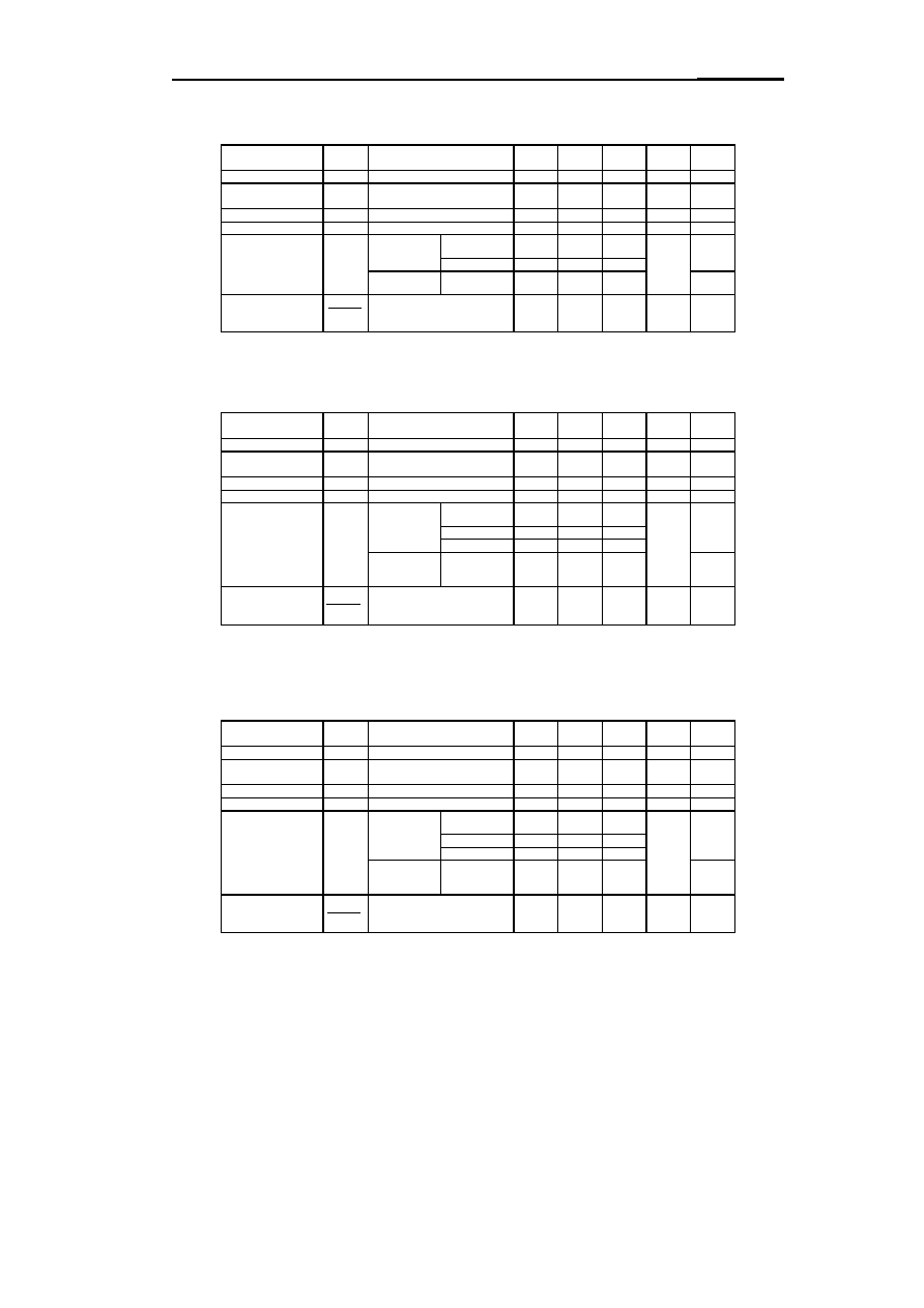
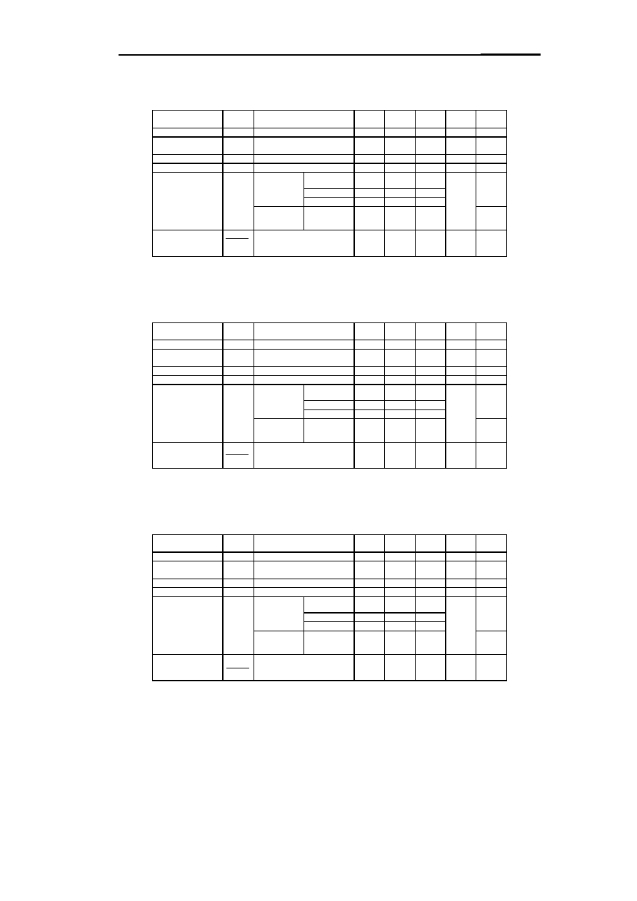
S-80715AL-AC-X, S-80715AN-DC-X (Detection voltage : 1.464 to 1.536 V)
(Unless otherwise specified : Ta=25
∞
C)
Parameter
Symbol
Conditions
Min.
Typ.
Max.
Unit
Test
circuit
Detection voltage
-V
DET
1.464
1.500
1.536
V
1
Hysteresis width
V
HYS
-V
DET
◊
0.02
-V
DET
◊
0.05
-V
DET
◊
0.08
V
1
Current consumption
I
SS
V
DD
= 3.0 V
1.4
3.5
µ
A
2
Operating voltage
V
DD
1.0
15.0
V
1
Output current
I
OUT
Nch
V
DS
= 0.5 V
V
DD
= 1.2 V
0.23
0.50
mA
3
Pch (CMOS
output)
V
DS
= 0.5 V
V
DD
= 4.8 V
0.36
0.62
4
Temperature
characteristic of -
V
DET
Ta=-30
∞
C to 80
∞
C
±
0.19
mV/
∞
C
2. S-80716AL-AD-X, S-80716AN/AN-DD-X (Detection voltage : 1.561 to 1.639 V)
(Unless otherwise specified : Ta=25
∞
C)
Parameter
Symbol
Conditions
Min.
Typ.
Max.
Unit
Test
circuit
Detection voltage
-V
DET
1.561
1.600
1.639
V
1
Hysteresis width
V
HYS
-V
DET
◊
0.02
-V
DET
◊
0.05
-V
DET
◊
0.08
V
1
Current consumption
I
SS
V
DD
= 3.0 V
1.4
3.5
µ
A
2
Operating voltage
V
DD
1.0
15.0
V
1
Output current
I
OUT
Nch
V
DS
= 0.5 V
V
DD
= 1.2 V
0.23
0.50
mA
3
Pch (CMOS
output)
V
DS
= 0.5 V
V
DD
= 4.8 V
0.36
0.62
4
Temperature
characteristic of -
V
DET
Ta=-30
∞
C to 80
∞
C
±
0.20
mV/
∞
C
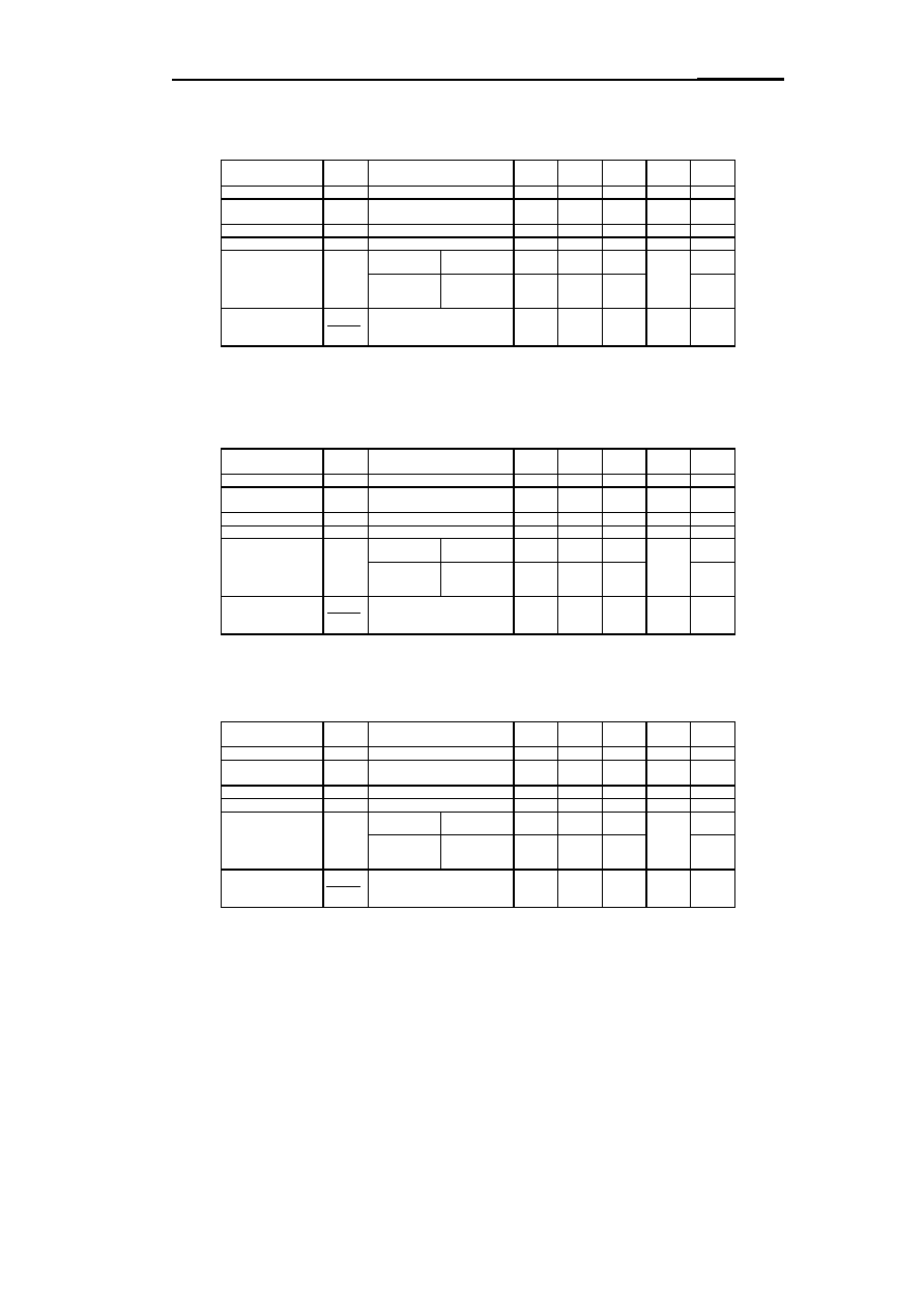
3.
S-80717AL/AL-AE-X, S-80717AN/AN-DE-X, S-80717SN-DE-X (Detection voltage : 1.659 to 1.741 V)
(Unless otherwise specified : Ta=25
∞
C)
Parameter
Symbol
Conditions
Min.
Typ.
Max.
Unit
Test
circuit
Detection voltage
-V
DET
1.659
1.700
1.741
V
1
Hysteresis width
V
HYS
-V
DET
◊
0.02
-V
DET
◊
0.05
-V
DET
◊
0.08
V
1
Current consumption
I
SS
V
DD
= 3.0 V
1.4
3.5
µ
A
2
Operating voltage
V
DD
1.0
15.0
V
1
Output current
I
OUT
Nch
V
DS
= 0.5 V
V
DD
= 1.2 V
0.23
0.50
mA
3
Pch (CMOS
output)
V
DS
= 0.5 V
V
DD
= 4.8 V
0.36
0.62
4
Temperature
characteristic of -
V
DET
Ta=-30
∞
C to 80
∞
C
±
0.21
mV/
∞
C
-V
DET
Ta
-V
DET
Ta
-V
DET
Ta
HIGH-PRECISION VOLTAGE DETECTOR
S-807 Series
8
Seiko Instruments Inc.
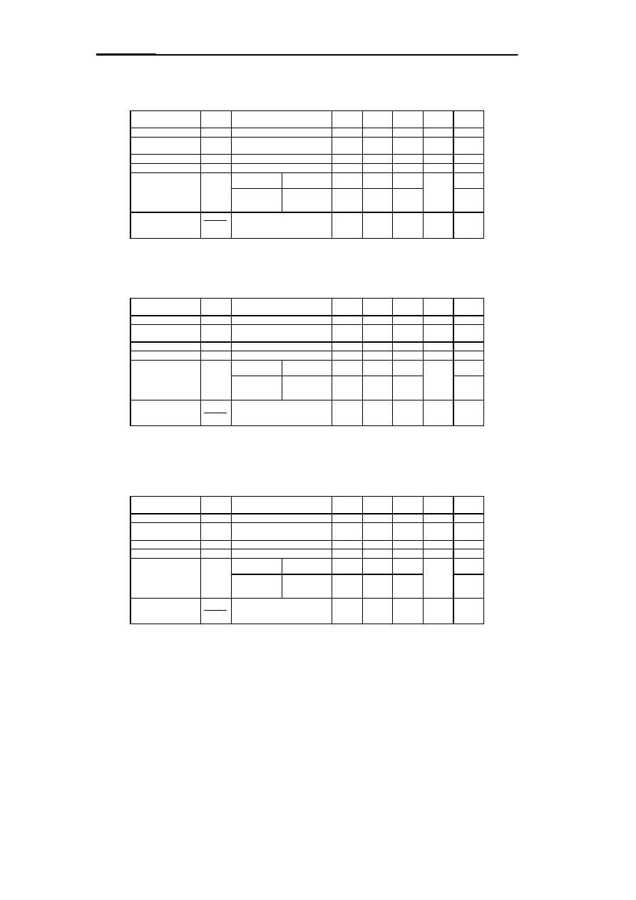
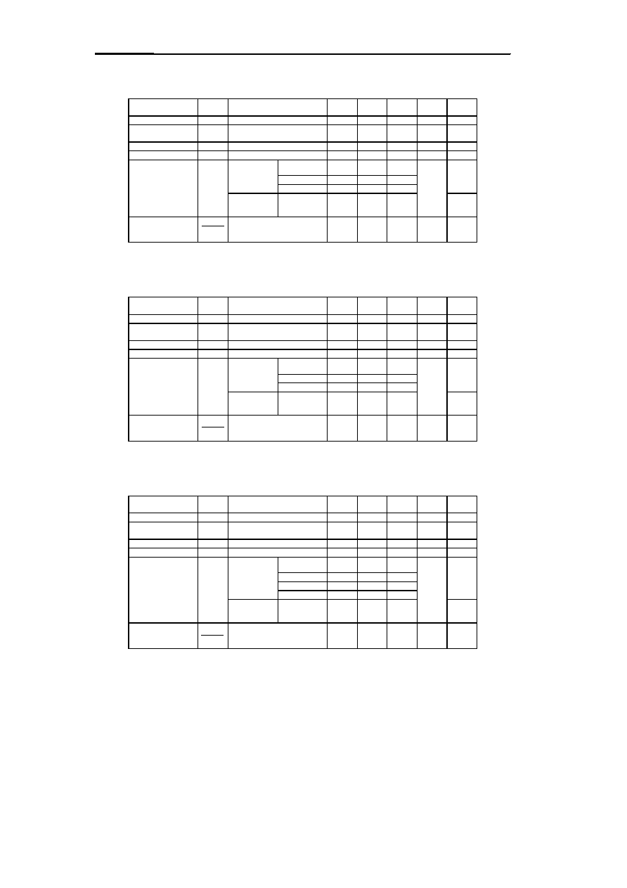
4. S-80718AL/AL-AF-X, S-80718AN/AN-DF-X, S-80718SL-AF-X (Detection voltage : 1.756 to 1.844 V)
(Unless otherwise specified : Ta=25
∞
C)
Parameter
Symbol
Conditions
Min.
Typ.
Max.
Unit
Test
circuit
Detection voltage
-V
DET
1.756
1.800
1.844
V
1
Hysteresis width
V
HYS
-V
DET
◊
0.02
-V
DET
◊
0.05
-V
DET
◊
0.08
V
1
Current consumption
I
SS
V
DD
= 3.0 V
1.4
3.5
µ
A
2
Operating voltage
V
DD
1.0
15.0
V
1
Output current
I
OUT
Nch
V
DS
= 0.5 V
V
DD
= 1.2 V
0.23
0.50
mA
3
Pch (CMOS
output)
V
DS
= 0.5 V
V
DD
= 4.8 V
0.36
0.62
4
Temperature
characteristic of -
V
DET
Ta=-30
∞
C to 80
∞
C
±
0.23
mV/
∞
C
5. S-80718AH-BF-T1 (Detection voltage : 1.756 to 1.844 V)
(Unless otherwise specified : Ta=25
∞
C)
Parameter
Symbol
Conditions
Min.
Typ.
Max.
Unit
Test
circuit
Detection voltage
-V
DET
1.756
1.800
1.844
V
1
Hysteresis width
V
HYS
-V
DET
◊
0.02
-V
DET
◊
0.05
-V
DET
◊
0.08
V
1
Current consumption
I
SS
V
DD
= 3.0 V
1.4
3.5
µ
A
2
Operating voltage
V
DD
1.0
15.0
V
1
Output current
I
OUT
Pch
V
DS
= 0.5 V
V
DD
= 1.2 V
0.03
0.09
mA
4
Nch
V
DS
= 0.5 V
V
DD
= 4.8 V
4.06
8.36
3
Temperature
characteristic of -
V
DET
Ta=-30
∞
C to 80
∞
C
±
0.23
mV/
∞
C
6.
S-80719AL/AL-AG-X, S-80719AN/AN-DG-X
S-80719SL-AG-X, S-80719SN-DG-X (Detection voltage : 1.854 to 1.946 V)
(Unless otherwise specified : Ta=25
∞
C)
Parameter
Symbol
Conditions
Min.
Typ.
Max.
Unit
Test
circuit
Detection voltage
-V
DET
1.854
1.900
1.946
V
1
Hysteresis width
V
HYS
-V
DET
◊
0.02
-V
DET
◊
0.05
-V
DET
◊
0.08
V
1
Current consumption
I
SS
V
DD
= 3.0 V
1.4
3.5
µ
A
2
Operating voltage
V
DD
1.0
15.0
V
1
Output current
I
OUT
Nch
V
DS
= 0.5 V
V
DD
= 1.2 V
0.23
0.50
mA
3
Pch (CMOS
output)
V
DS
= 0.5 V
V
DD
= 4.8 V
0.36
0.62
4
Temperature
characteristic of -
V
DET
Ta=-30
∞
C to 80
∞
C
±
0.24
mV/
∞
C
-V
DET
Ta
-V
DET
Ta
-V
DET
Ta
HIGH-PRECISION VOLTAGE DETECTOR
S-807 Series
Seiko Instruments Inc.
9
7.
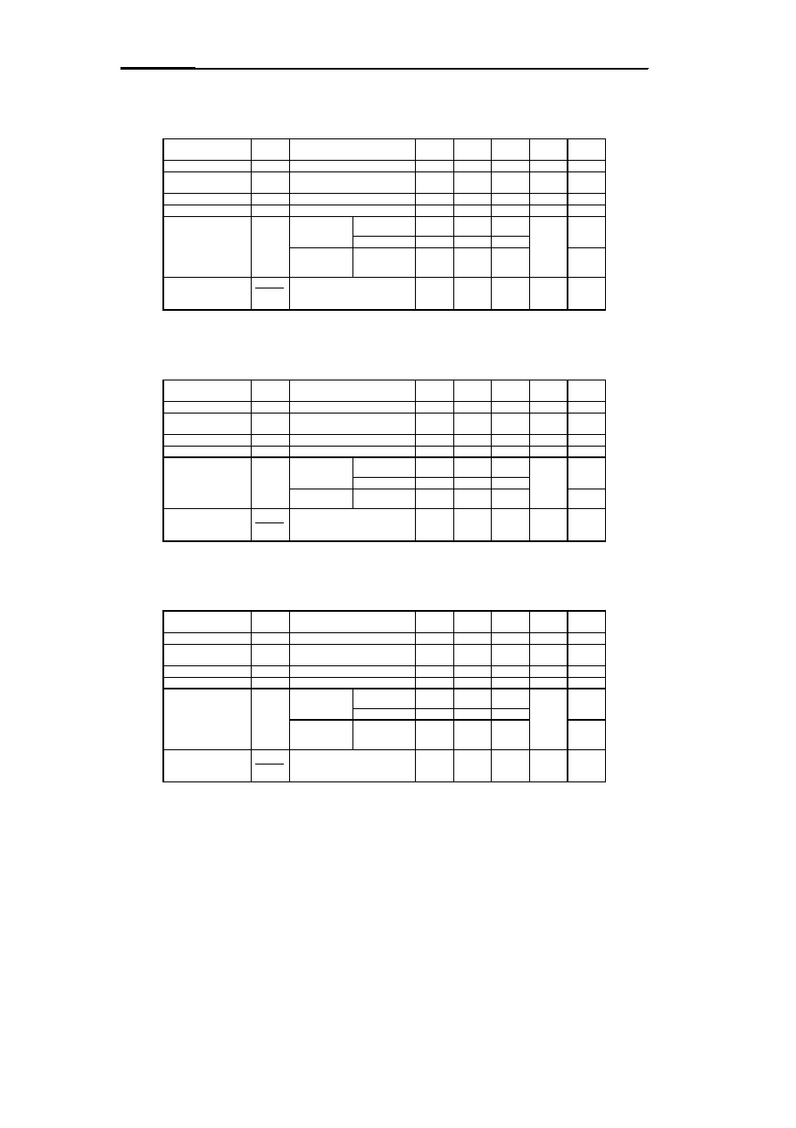
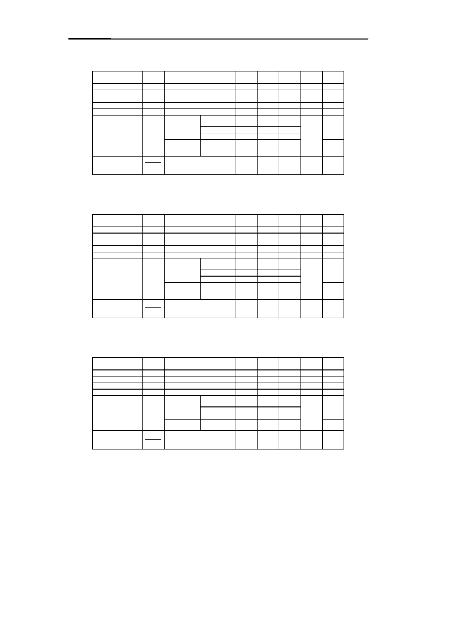
S-80720AL-AH-X, S-80720AN/AN-DH-X
S-80720SL-AH-X, S-80720SN-DH-X (Detection voltage : 1.952 to 2.048 V)
(Unless otherwise specified : Ta=25
∞
C)
Parameter
Symbol
Conditions
Min.
Typ.
Max.
Unit
Test
circuit
Detection voltage
-V
DET
1.952
2.000
2.048
V
1
Hysteresis width
V
HYS
-V
DET
◊
0.02
-V
DET
◊
0.05
-V
DET
◊
0.08
V
1
Current consumption
I
SS
V
DD
= 3.0 V
1.4
3.5
µ
A
2
Operating voltage
V
DD
1.0
15.0
V
1
Output current
I
OUT
Nch
V
DS
= 0.5 V
V
DD
= 1.2 V
0.23
0.50
mA
3
Pch (CMOS
output)
V
DS
= 0.5 V
V
DD
= 4.8 V
0.36
0.62
4
Temperature
characteristic of -
V
DET
Ta=-30
∞
C to 80
∞
C
±
0.25
mV/
∞
C
8.
S-80721AL/AL-AJ-X, S-80721AN/AN-DJ-X
S-80721SL-AJ-X, S-80721SN-DJ-X (Detection voltage : 2.049 to 2.151 V)
(Unless otherwise specified : Ta=25
∞
C)
Parameter
Symbol
Conditions
Min.
Typ.
Max.
Unit
Test
circuit
Detection voltage
-V
DET
2.049
2.100
2.151
V
1
Hysteresis width
V
HYS
-V
DET
◊
0.02
-V
DET
◊
0.05
-V
DET
◊
0.08
V
1
Current consumption
I
SS
V
DD
= 4.5 V
1.4
3.5
µ
A
2
Operating voltage
V
DD
1.0
15.0
V
1
Output current
I
OUT
Nch
V
DS
= 0.5 V
V
DD
= 1.2 V
0.23
0.50
mA
3
Pch (CMOS
output)
V
DS
= 0.5 V
V
DD
= 4.8 V
0.36
0.62
4
Temperature
characteristic of -
V
DET
Ta=-30
∞
C to 80
∞
C
±
0.26
mV/
∞
C
9.
S-80722AL/AL-AK-X, S-80722AN/AN-DK-X (Detection voltage : 2.147 to 2.253 V)
(Unless otherwise specified : Ta=25
∞
C)
Parameter
Symbol
Conditions
Min.
Typ.
Max.
Unit
Test
circuit
Detection voltage
-V
DET
2.147
2.200
2.253
V
1
Hysteresis width
V
HYS
-V
DET
◊
0.02
-V
DET
◊
0.05
-V
DET
◊
0.08
V
1
Current consumption
I
SS
V
DD
= 4.5 V
1.4
3.5
µ
A
2
Operating voltage
V
DD
1.0
15.0
V
1
Output current
I
OUT
Nch
V
DS
= 0.5 V
V
DD
= 1.2 V
0.23
0.50
mA
3
Pch (CMOS
output)
V
DS
= 0.5 V
V
DD
= 4.8 V
0.36
0.62
4
Temperature
characteristic of -
V
DET
Ta=-30
∞
C to 80
∞
C
±
0.28
mV/
∞
C
-V
DET
Ta
-V
DET
Ta
-V
DET
Ta
HIGH-PRECISION VOLTAGE DETECTOR
S-807 Series
10
Seiko Instruments Inc.
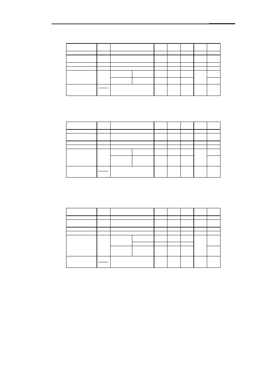
10. S-80723AL/AL-AL-X, S-80723AN/AN-DL-X
S-80723SL-AL-X, S-80723SN-DL-X (Detection voltage : 2.244 to 2.356 V)
(Unless otherwise specified : Ta=25
∞
C)
Parameter
Symbol
Conditions
Min.
Typ.
Max.
Unit
Test
circuit
Detection voltage
-V
DET
2.244
2.300
2.356
V
1
Hysteresis width
V
HYS
-V
DET
◊
0.02
-V
DET
◊
0.05
-V
DET
◊
0.08
V
1
Current consumption
I
SS
V
DD
= 4.5 V
1.4
3.5
µ
A
2
Operating voltage
V
DD
1.0
15.0
V
1
Output current
I
OUT
Nch
V
DS
= 0.5 V
V
DD
= 1.2 V
0.23
0.50
mA
3
Pch (CMOS
output)
V
DS
= 0.5 V
V
DD
= 4.8 V
0.36
0.62
4
Temperature
characteristic of -
V
DET
Ta=-30
∞
C to 80
∞
C
±
0.29
mV/
∞
C
11. S-80724AL/AL-AM-X, S-80724AN/AN-DM-X, S-80724SN-DM-X (Detection voltage : 2.342 to 2.458 V)
(Unless otherwise specified : Ta=25
∞
C)
Parameter
Symbol
Conditions
Min.
Typ.
Max.
Unit
Test
circuit
Detection voltage
-V
DET
2.342
2.400
2.458
V
1
Hysteresis width
V
HYS
-V
DET
◊
0.02
-V
DET
◊
0.05
-V
DET
◊
0.08
V
1
Current consumption
I
SS
V
DD
= 4.5 V
1.4
3.5
µ
A
2
Operating voltage
V
DD
1.0
15.0
V
1
Output current
I
OUT
Nch
V
DS
= 0.5 V
V
DD
= 1.2 V
0.23
0.50
mA
3
Pch (CMOS
output)
V
DS
= 0.5 V
V
DD
= 4.8 V
0.36
0.62
4
Temperature
characteristic of -
V
DET
Ta=-30
∞
C to 80
∞
C
±
0.30
mV/
∞
C
12. S-80725AL/AL-AN-X, S-80725AN/AN-DN-X
S-80725SL-AN-X, S-80725SN-DN-X (Detection voltage : 2.440 to 2.560 V)
(Unless otherwise specified : Ta=25
∞
C)
Parameter
Symbol
Conditions
Min.
Typ.
Max.
Unit
Test
circuit
Detection voltage
-V
DET
2.440
2.500
2.560
V
1
Hysteresis width
V
HYS
-V
DET
◊
0.02
-V
DET
◊
0.05
-V
DET
◊
0.08
V
1
Current consumption
I
SS
V
DD
= 4.5 V
1.4
3.5
µ
A
2
Operating voltage
V
DD
1.0
15.0
V
1
Output current
I
OUT
Nch
V
DS
= 0.5 V
V
DD
= 1.2 V
0.23
0.50
mA
3
Pch (CMOS
output)
V
DS
= 0.5 V
V
DD
= 4.8 V
0.36
0.62
4
Temperature
characteristic of -
V
DET
Ta=-30
∞
C to 80
∞
C
±
0.31
mV/
∞
C
-V
DET
Ta
-V
DET
Ta
-V
DET
Ta
HIGH-PRECISION VOLTAGE DETECTOR
S-807 Series
Seiko Instruments Inc.
11
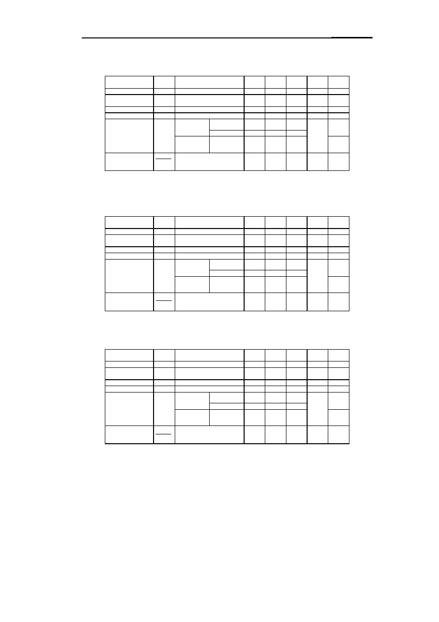
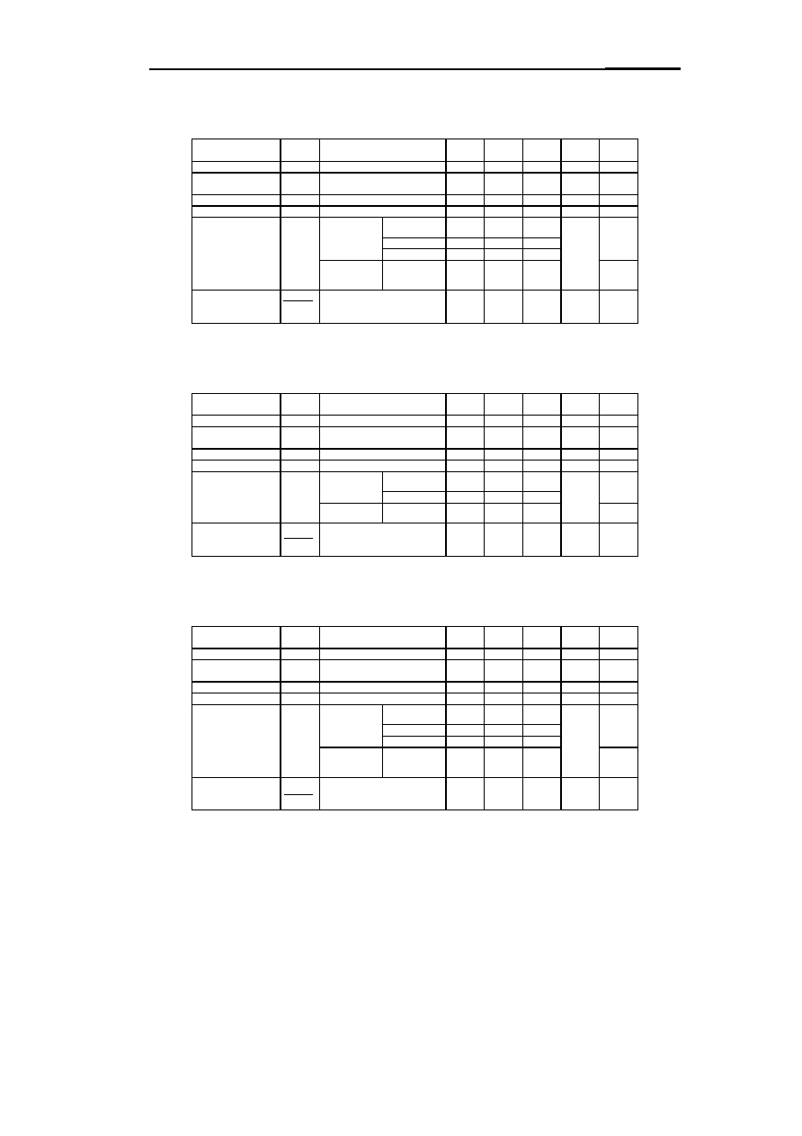
13. S-80725AH-BN-X (Detection voltage : 2.440 to 2.560 V)
(Unless otherwise specified : Ta=25
∞
C)
Parameter
Symbol
Conditions
Min.
Typ.
Max.
Unit
Test
circuit
Detection voltage
-V
DET
2.440
2.500
2.560
V
1
Hysteresis width
V
HYS
-V
DET
◊
0.02
-V
DET
◊
0.05
-V
DET
◊
0.08
V
1
Current consumption
I
SS
V
DD
= 4.5 V
1.4
3.5
µ
A
2
Operating voltage
V
DD
1.0
15.0
V
1
Output current
I
OUT
Pch
V
DS
= 0.5 V
V
DD
= 1.2 V
0.03
0.09
mA
4
Nch
V
DS
= 0.5 V
V
DD
= 4.8 V
4.06
8.36
3
Temperature
characteristic of -
V
DET
Ta=-30
∞
C to 80
∞
C
±
0.31
mV/
∞
C
14. S-80726AL-AP-X, S-80726AN/AN-DP-X (Detection voltage : 2.537 to 2.663 V)
(Unless otherwise specified : Ta=25
∞
C)
Parameter
Symbol
Conditions
Min.
Typ.
Max.
Unit
Test
circuit
Detection voltage
-V
DET
2.537
2.600
2.663
V
1
Hysteresis width
V
HYS
-V
DET
◊
0.02
-V
DET
◊
0.05
-V
DET
◊
0.08
V
1
Current consumption
I
SS
V
DD
= 4.5 V
1.0
3.0
µ
A
2
Operating voltage
V
DD
1.0
15.0
V
1
Output current
I
OUT
Nch
V
DS
= 0.5 V
V
DD
= 1.2 V
0.23
0.50
mA
3
Pch (CMOS
output)
V
DS
= 0.5 V
V
DD
= 4.8 V
0.36
0.62
4
Temperature
characteristic of -
V
DET
Ta=-30
∞
C to 80
∞
C
±
0.33
mV/
∞
C
15. S-80727AL/AL-AQ-X, S-80727AN/AN-DQ-X
S-80727SL-AQ-X, S-80727SN-DQ-X (Detection voltage : 2.635 to 2.765 V)
(Unless otherwise specified : Ta=25
∞
C)
Parameter
Symbol
Conditions
Min.
Typ.
Max.
Unit
Test
circuit
Detection voltage
-V
DET
2.635
2.700
2.765
V
1
Hysteresis width
V
HYS
-V
DET
◊
0.02
-V
DET
◊
0.05
-V
DET
◊
0.08
V
1
Current consumption
I
SS
V
DD
= 4.5 V
1.0
3.0
µ
A
2
Operating voltage
V
DD
1.0
15.0
V
1
Output current
I
OUT
Nch
V
DS
= 0.5 V
V
DD
= 1.2 V
0.23
0.50
mA
3
V
DD
= 2.4 V
1.60
3.70
Pch (CMOS
output)
V
DS
= 0.5 V
V
DD
= 4.8 V
0.36
0.62
4
Temperature
characteristic of -
V
DET
Ta=-30
∞
C to 80
∞
C
±
0.34
mV/
∞
C
-V
DET
Ta
-V
DET
Ta
-V
DET
Ta
HIGH-PRECISION VOLTAGE DETECTOR
S-807 Series
12
Seiko Instruments Inc.
16. S-80728AL-AR-X, S-80728AN/AN-DR-X
S-80728SL-AR-X, S-80728SN-DR-X (Detection voltage : 2.732 to 2.868 V)
(Unless otherwise specified : Ta=25
∞
C)
Parameter
Symbol
Conditions
Min.
Typ.
Max.
Unit
Test
circuit
Detection voltage
-V
DET
2.732
2.800
2.868
V
1
Hysteresis width
V
HYS
-V
DET
◊
0.02
-V
DET
◊
0.05
-V
DET
◊
0.08
V
1
Current consumption
I
SS
V
DD
= 4.5 V
1.0
3.0
µ
A
2
Operating voltage
V
DD
1.0
15.0
V
1
Output current
I
OUT
Nch
V
DS
= 0.5 V
V
DD
= 1.2 V
0.23
0.50
mA
3
V
DD
= 2.4 V
1.60
3.70
Pch (CMOS
output)
V
DS
= 0.5 V
V
DD
= 4.8 V
0.36
0.62
4
Temperature
characteristic of -
V
DET
Ta=-30
∞
C to 80
∞
C
±
0.35
mV/
∞
C
17. S-80729AL/AL-AS-X, S-80729AN-DS-X (Detection voltage : 2.830 to 2.970 V)
(Unless otherwise specified : Ta=25
∞
C)
Parameter
Symbol
Conditions
Min.
Typ.
Max.
Unit
Test
circuit
Detection voltage
-V
DET
2.830
2.900
2.970
V
1
Hysteresis width
V
HYS
-V
DET
◊
0.02
-V
DET
◊
0.05
-V
DET
◊
0.08
V
1
Current consumption
I
SS
V
DD
= 4.5 V
1.0
3.0
µ
A
2
Operating voltage
V
DD
1.0
15.0
V
1
Output current
I
OUT
Nch
V
DS
= 0.5 V
V
DD
= 1.2 V
0.23
0.50
mA
3
V
DD
= 2.4 V
1.60
3.70
Pch (CMOS
output)
V
DS
= 0.5 V
V
DD
= 4.8 V
0.36
0.62
4
Temperature
characteristic of -
V
DET
Ta=-30
∞
C to 80
∞
C
±
0.36
mV/
∞
C
18. S-80730AL/AL-AT-X, S-80730AN/AN-DT-X
S-80730SL-AT-X, S-80730SN-DT-X (Detection voltage : 2.928 to 3.072 V)
(Unless otherwise specified : Ta=25
∞
C)
Parameter
Symbol
Conditions
Min.
Typ.
Max.
Unit
Test
circuit
Detection voltage
-V
DET
2.928
3.000
3.072
V
1
Hysteresis width
V
HYS
-V
DET
◊
0.02
-V
DET
◊
0.05
-V
DET
◊
0.08
V
1
Current consumption
I
SS
V
DD
= 4.5 V
1.0
3.0
µ
A
2
Operating voltage
V
DD
1.0
15.0
V
1
Output current
I
OUT
Nch
V
DS
= 0.5 V
V
DD
= 1.2 V
0.23
0.50
mA
3
V
DD
= 2.4 V
1.60
3.70
Pch (CMOS
output)
V
DS
= 0.5 V
V
DD
= 4.8 V
0.36
0.62
4
Temperature
characteristic of -
V
DET
Ta=-30
∞
C to 80
∞
C
±
0.38
mV/
∞
C
-V
DET
Ta
-V
DET
Ta
-V
DET
Ta
HIGH-PRECISION VOLTAGE DETECTOR
S-807 Series
Seiko Instruments Inc.
13
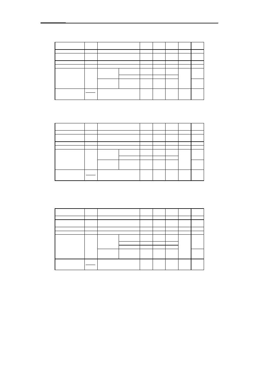
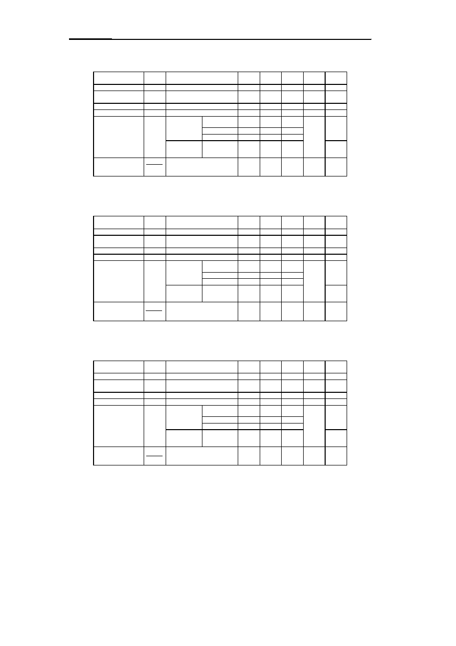
19. S-80731AL/AL-AV-X, S-80731AN/AN-DV-X (Detection voltage : 3.025 to 3.175 V)
(Unless otherwise specified : Ta=25
∞
C)
Parameter
Symbol
Conditions
Min.
Typ.
Max.
Unit
Test
circuit
Detection voltage
-V
DET
3.025
3.100
3.175
V
1
Hysteresis width
V
HYS
-V
DET
◊
0.02
-V
DET
◊
0.05
-V
DET
◊
0.08
V
1
Current consumption
I
SS
V
DD
= 4.5 V
1.0
3.0
µ
A
2
Operating voltage
V
DD
1.0
15.0
V
1
Output current
I
OUT
Nch
V
DS
= 0.5 V
V
DD
= 1.2 V
0.23
0.50
mA
3
V
DD
= 2.4 V
1.60
3.70
Pch (CMOS
output)
V
DS
= 0.5 V
V
DD
= 4.8 V
0.36
0.62
4
Temperature
characteristic of -
V
DET
Ta=-30
∞
C to 80
∞
C
±
0.39
mV/
∞
C
20. S-80731AH/AH-BV-X (Detection voltage : 3.025 to 3.175 V)
(Unless otherwise specified : Ta=25
∞
C)
Parameter
Symbol
Conditions
Min.
Typ.
Max.
Unit
Test
circuit
Detection voltage
-V
DET
3.025
3.100
3.175
V
1
Hysteresis width
V
HYS
-V
DET
◊
0.02
-V
DET
◊
0.05
-V
DET
◊
0.08
V
1
Current consumption
I
SS
V
DD
= 4.5 V
1.0
3.0
µ
A
2
Operating voltage
V
DD
1.0
15.0
V
1
Output current
I
OUT
Pch
V
DS
= 0.5 V
V
DD
= 1.2 V
0.03
0.09
mA
4
V
DD
= 2.4 V
0.15
0.30
Nch
V
DS
= 0.5 V
V
DD
= 4.8 V
4.06
8.36
3
Temperature
characteristic of -
V
DET
Ta=-30
∞
C to 80
∞
C
±
0.39
mV/
∞
C
21. S-80732AL/AL-AW-X, S-80732AN/AN-DW-X, S-80732SL-AW-X (Detection voltage : 3.123 to 3.277 V)
(Unless otherwise specified : Ta=25
∞
C)
Parameter
Symbol
Conditions
Min.
Typ.
Max.
Unit
Test
circuit
Detection voltage
-V
DET
3.123
3.200
3.277
V
1
Hysteresis width
V
HYS
-V
DET
◊
0.02
-V
DET
◊
0.05
-V
DET
◊
0.08
V
1
Current consumption
I
SS
V
DD
= 4.5 V
1.0
3.0
µ
A
2
Operating voltage
V
DD
1.0
15.0
V
1
Output current
I
OUT
Nch
V
DS
= 0.5 V
V
DD
= 1.2 V
0.23
0.50
mA
3
V
DD
= 2.4 V
1.60
3.70
Pch (CMOS
output)
V
DS
= 0.5 V
V
DD
= 4.8 V
0.36
0.62
4
Temperature
characteristic of -
V
DET
Ta=-30
∞
C to 80
∞
C
±
0.40
mV/
∞
C
-V
DET
Ta
-V
DET
Ta
-V
DET
Ta
HIGH-PRECISION VOLTAGE DETECTOR
S-807 Series
14
Seiko Instruments Inc.
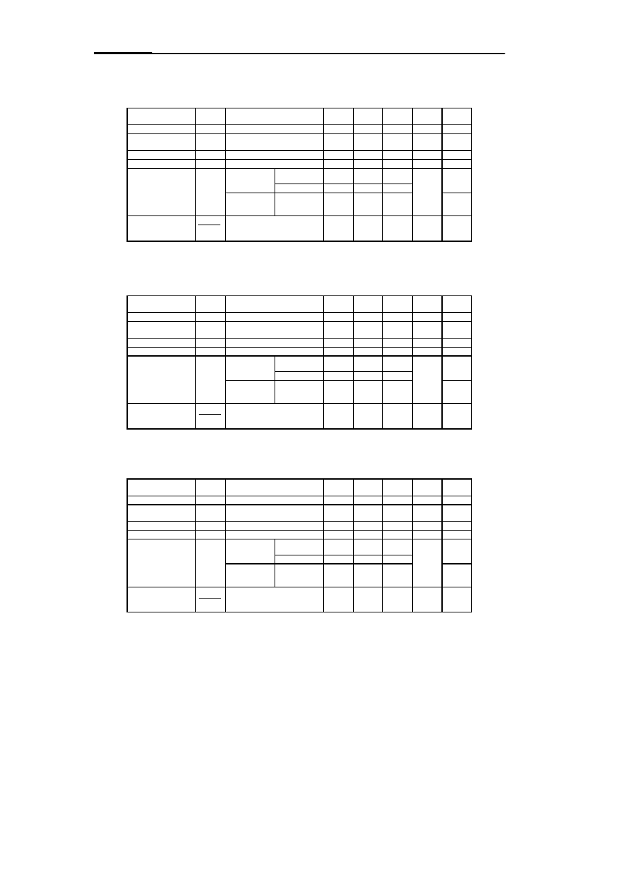
22. S-80733AL/AL-AX-X, S-80733AN/AN-DX-X
S-80733SL-AX-X, S-80733SN-DX-X (Detection voltage : 3.220 to 3.380 V)
(Unless otherwise specified : Ta=25
∞
C)
Parameter
Symbol
Conditions
Min.
Typ.
Max.
Unit
Test
circuit
Detection voltage
-V
DET
3.220
3.300
3.380
V
1
Hysteresis width
V
HYS
-V
DET
◊
0.02
-V
DET
◊
0.05
-V
DET
◊
0.08
V
1
Current consumption
I
SS
V
DD
= 4.5 V
1.0
3.0
µ
A
2
Operating voltage
V
DD
1.0
15.0
V
1
Output current
I
OUT
Nch
V
DS
= 0.5 V
V
DD
= 1.2 V
0.23
0.50
mA
3
V
DD
= 2.4 V
1.60
3.70
Pch (CMOS
output)
V
DS
= 0.5 V
V
DD
= 4.8 V
0.36
0.62
4
Temperature
characteristic of -
V
DET
Ta=-30
∞
C to 80
∞
C
±
0.41
mV/
∞
C
23. S-80733AH (Detection voltage : 3.220 to 3.380 V)
(Unless otherwise specified : Ta=25
∞
C)
Parameter
Symbol
Conditions
Min.
Typ.
Max.
Unit
Test
circuit
Detection voltage
-V
DET
3.220
3.300
3.380
V
1
Hysteresis width
V
HYS
-V
DET
◊
0.02
-V
DET
◊
0.05
-V
DET
◊
0.08
V
1
Current consumption
I
SS
V
DD
= 4.5 V
1.0
3.0
µ
A
2
Operating voltage
V
DD
1.0
15.0
V
1
Output current
I
OUT
Pch
V
DS
= 0.5 V
V
DD
= 1.2 V
0.03
0.09
mA
4
V
DD
= 2.4 V
0.15
0.30
Nch
V
DS
= 0.5 V
V
DD
= 4.8 V
4.06
8.36
3
Temperature
characteristic of -
V
DET
Ta=-30
∞
C to 80
∞
C
±
0.41
mV/
∞
C
24. S-80734AL/AL-AY-X, S-80734AN/AN-DY-X (Detection voltage : 3.318 to 3.482 V)
(Unless otherwise specified : Ta=25
∞
C)
Parameter
Symbol
Conditions
Min.
Typ.
Max.
Unit
Test
circuit
Detection voltage
-V
DET
3.318
3.400
3.482
V
1
Hysteresis width
V
HYS
-V
DET
◊
0.02
-V
DET
◊
0.05
-V
DET
◊
0.08
V
1
Current consumption
I
SS
V
DD
= 4.5 V
1.0
3.0
µ
A
2
Operating voltage
V
DD
1.0
15.0
V
1
Output current
I
OUT
Nch
V
DS
= 0.5 V
V
DD
= 1.2 V
0.23
0.50
mA
3
V
DD
= 2.4 V
1.60
3.70
Pch (CMOS
output)
V
DS
= 0.5 V
V
DD
= 4.8 V
0.36
0.62
4
Temperature
characteristic of -
V
DET
Ta=-30
∞
C to 80
∞
C
±
0.43
mV/
∞
C
-V
DET
Ta
-V
DET
Ta
-V
DET
Ta
HIGH-PRECISION VOLTAGE DETECTOR
S-807 Series
Seiko Instruments Inc.
15
25. S-80735AL/AL-AZ-X, S-80735AN/AN-DZ-X
S-80735SL-AZ-X, S-80735SN-DZ-X (Detection voltage : 3.416 to 3.584 V)
(Unless otherwise specified : Ta=25
∞
C)
Parameter
Symbol
Conditions
Min.
Typ.
Max.
Unit
Test
circuit
Detection voltage
-V
DET
3.416
3.500
3.584
V
1
Hysteresis width
V
HYS
-V
DET
◊
0.02
-V
DET
◊
0.05
-V
DET
◊
0.08
V
1
Current consumption
I
SS
V
DD
= 4.5 V
1.0
3.0
µ
A
2
Operating voltage
V
DD
1.0
15.0
V
1
Output current
I
OUT
Nch
V
DS
= 0.5 V
V
DD
= 1.2 V
0.23
0.50
mA
3
V
DD
= 2.4 V
1.60
3.70
Pch (CMOS
output)
V
DS
= 0.5 V
V
DD
= 4.8 V
0.36
0.62
4
Temperature
characteristic of -
V
DET
Ta=-30
∞
C to 80
∞
C
±
0.44
mV/
∞
C
26. S-80736AL-A0-X, S-80736AN/AN-D0-X (Detection voltage : 3.513 to 3.687 V)
(Unless otherwise specified : Ta=25
∞
C)
Parameter
Symbol
Conditions
Min.
Typ.
Max.
Unit
Test
circuit
Detection voltage
-V
DET
3.513
3.600
3.687
V
1
Hysteresis width
V
HYS
-V
DET
◊
0.02
-V
DET
◊
0.05
-V
DET
◊
0.08
V
1
Current consumption
I
SS
V
DD
= 4.5 V
1.0
3.0
µ
A
2
Operating voltage
V
DD
1.0
15.0
V
1
Output current
I
OUT
Nch
V
DS
= 0.5 V
V
DD
= 1.2 V
0.23
0.50
mA
3
V
DD
= 2.4 V
1.60
3.70
Pch (CMOS
output)
V
DS
= 0.5 V
V
DD
= 4.8 V
0.36
0.62
4
Temperature
characteristic of -
V
DET
Ta=-30
∞
C to 80
∞
C
±
0.45
mV/
∞
C
27. S-80737AL/AL-A1-X, S-80737AN/AN-D1-X (Detection voltage : 3.611 to 3.789 V)
(Unless otherwise specified : Ta=25
∞
C)
Parameter
Symbol
Conditions
Min.
Typ.
Max.
Unit
Test
circuit
Detection voltage
-V
DET
3.611
3.700
3.789
V
1
Hysteresis width
V
HYS
-V
DET
◊
0.02
-V
DET
◊
0.05
-V
DET
◊
0.08
V
1
Current consumption
I
SS
V
DD
= 6.0 V
1.0
3.0
µ
A
2
Operating voltage
V
DD
1.0
15.0
V
1
Output current
I
OUT
Nch
V
DS
= 0.5 V
V
DD
= 1.2 V
0.23
0.50
mA
3
V
DD
= 2.4 V
1.60
3.70
Pch (CMOS
output)
V
DS
= 0.5 V
V
DD
= 4.8 V
0.36
0.62
4
Temperature
characteristic of -
V
DET
Ta=-30
∞
C to 80
∞
C
±
0.46
mV/
∞
C
-V
DET
Ta
-V
DET
Ta
-V
DET
Ta
HIGH-PRECISION VOLTAGE DETECTOR
S-807 Series
16
Seiko Instruments Inc.
28. S-80738AL/AL-A2-X, S-80738AN/AN-D2-X (Detection voltage : 3.708 to 3.892 V)
(Unless otherwise specified : Ta=25
∞
C)
Parameter
Symbol
Conditions
Min.
Typ.
Max.
Unit
Test
circuit
Detection voltage
-V
DET
3.708
3.800
3.892
V
1
Hysteresis width
V
HYS
-V
DET
◊
0.02
-V
DET
◊
0.05
-V
DET
◊
0.08
V
1
Current consumption
I
SS
V
DD
= 6.0 V
1.0
3.0
µ
A
2
Operating voltage
V
DD
1.0
15.0
V
1
Output current
I
OUT
Nch
V
DS
= 0.5 V
V
DD
= 1.2 V
0.23
0.50
mA
3
V
DD
= 2.4 V
1.60
3.70
Pch (CMOS
output)
V
DS
= 0.5 V
V
DD
= 4.8 V
0.36
0.62
4
Temperature
characteristic of -
V
DET
Ta=-30
∞
C to 80
∞
C
±
0.48
mV/
∞
C
29. S-80739AL/AL-A3-X, S-80739AN/AN-D3-X (Detection voltage : 3.806 to 3.994 V)
(Unless otherwise specified : Ta=25
∞
C)
Parameter
Symbol
Conditions
Min.
Typ.
Max.
Unit
Test
circuit
Detection voltage
-V
DET
3.806
3.900
3.994
V
1
Hysteresis width
V
HYS
-V
DET
◊
0.02
-V
DET
◊
0.05
-V
DET
◊
0.08
V
1
Current consumption
I
SS
V
DD
= 6.0 V
1.0
3.0
µ
A
2
Operating voltage
V
DD
1.0
15.0
V
1
Output current
I
OUT
Nch
V
DS
= 0.5 V
V
DD
= 1.2 V
0.23
0.50
mA
3
V
DD
= 2.4 V
1.60
3.70
Pch (CMOS
output)
V
DS
= 0.5 V
V
DD
= 4.8 V
0.36
0.62
4
Temperature
characteristic of -
V
DET
Ta=-30
∞
C to 80
∞
C
±
0.49
mV/
∞
C
30. S-80740AL/AL-A4-X, S-80740AN/AN-D4-X
S-80740SL-A4-X, S-80740SN-D4-X (Detection voltage : 3.904 to 4.096 V)
(Unless otherwise specified : Ta=25
∞
C)
Parameter
Symbol
Conditions
Min.
Typ.
Max.
Unit
Test
circuit
Detection voltage
-V
DET
3.904
4.00
4.096
V
1
Hysteresis width
V
HYS
-V
DET
◊
0.02
-V
DET
◊
0.05
-V
DET
◊
0.08
V
1
Current consumption
I
SS
V
DD
= 6.0 V
1.0
3.0
µ
A
2
Operating voltage
V
DD
1.0
15.0
V
1
Output current
I
OUT
Nch
V
DS
= 0.5 V
V
DD
= 1.2 V
0.23
0.50
mA
3
V
DD
= 2.4 V
1.60
3.70
V
DD
= 3.6 V
3.18
7.00
Pch (CMOS
output)
V
DS
= 0.5 V
V
DD
= 6.0 V
0.46
0.75
4
Temperature
characteristic of -
V
DET
Ta=-30
∞
C to 80
∞
C
±
0.5
mV/
∞
C
-V
DET
Ta
-V
DET
Ta
-V
DET
Ta
HIGH-PRECISION VOLTAGE DETECTOR
S-807 Series
Seiko Instruments Inc.
17
31. S-80740AH/AH-B4-X (Detection voltage : 3.904 to 4.096 V)
(Unless otherwise specified : Ta=25
∞
C)
Parameter
Symbol
Conditions
Min.
Typ.
Max.
Unit
Test
circuit
Detection voltage
-V
DET
3.904
4.000
4.096
V
1
Hysteresis width
V
HYS
-V
DET
◊
0.02
-V
DET
◊
0.05
-V
DET
◊
0.08
V
1
Current consumption
I
SS
V
DD
= 6.0 V
1.0
3.0
µ
A
2
Operating voltage
V
DD
1.0
15.0
V
1
Output current
I
OUT
Pch
V
DS
= 0.5 V
V
DD
= 1.2 V
0.03
0.09
mA
4
V
DD
= 2.4 V
0.15
0.30
Nch
V
DS
= 0.5 V
V
DD
= 6.0 V
4.73
9.60
3
Temperature
characteristic of -
V
DET
Ta=-30
∞
C to 80
∞
C
±
0.5
mV/
∞
C
32. S-80741AL/AL-A5-X, S-80741AN/AN-D5-X (Detection voltage : 4.001 to 4.199 V)
(Unless otherwise specified : Ta=25
∞
C)
Parameter
Symbol
Conditions
Min.
Typ.
Max.
Unit
Test
circuit
Detection voltage
-V
DET
4.001
4.100
4.199
V
1
Hysteresis width
V
HYS
-V
DET
◊
0.02
-V
DET
◊
0.05
-V
DET
◊
0.08
V
1
Current consumption
I
SS
V
DD
= 6.0 V
1.0
3.0
µ
A
2
Operating voltage
V
DD
1.0
15.0
V
1
Output current
I
OUT
Nch
V
DS
= 0.5 V
V
DD
= 1.2 V
0.23
0.50
mA
3
V
DD
= 2.4 V
1.60
3.70
V
DD
= 3.6 V
3.18
7.00
Pch (CMOS
output)
V
DS
= 0.5 V
V
DD
= 6.0 V
0.46
0.75
4
Temperature
characteristic of -
V
DET
Ta=-30
∞
C to 80
∞
C
±
0.51
mV/
∞
C
33. S-80742AL/AL-A6-X, S-80742AN/AN-D6-X
S-80742SL-A6-X, S-80742SN-D6-X (Detection voltage : 4.099 to 4.301 V)
(Unless otherwise specified : Ta=25
∞
C)
Parameter
Symbol
Conditions
Min.
Typ.
Max.
Unit
Test
circuit
Detection voltage
-V
DET
4.099
4.200
4.301
V
1
Hysteresis width
V
HYS
-V
DET
◊
0.02
-V
DET
◊
0.05
-V
DET
◊
0.08
V
1
Current consumption
I
SS
V
DD
= 6.0 V
1.0
3.0
µ
A
2
Operating voltage
V
DD
1.0
15.0
V
1
Output current
I
OUT
Nch
V
DS
= 0.5 V
V
DD
= 1.2 V
0.23
0.50
mA
3
V
DD
= 2.4 V
1.60
3.70
V
DD
= 3.6 V
3.18
7.00
Pch (CMOS
output)
V
DS
= 0.5 V
V
DD
= 6.0 V
0.46
0.75
4
Temperature
characteristic of -
V
DET
Ta=-30
∞
C to 80
∞
C
±
0.53
mV/
∞
C
-V
DET
Ta
-V
DET
Ta
-V
DET
Ta
HIGH-PRECISION VOLTAGE DETECTOR
S-807 Series
18
Seiko Instruments Inc.
34. S-80743AL/AL-A7-X, S-80743AN/AN-D7-X (Detection voltage : 4.196 to 4.404 V)
(Unless otherwise specified : Ta=25
∞
C)
Parameter
Symbol
Conditions
Min.
Typ.
Max.
Unit
Test
circuit
Detection voltage
-V
DET
4.196
4.300
4.404
V
1
Hysteresis width
V
HYS
-V
DET
◊
0.02
-V
DET
◊
0.05
-V
DET
◊
0.08
V
1
Current consumption
I
SS
V
DD
= 6.0 V
1.0
3.0
µ
A
2
Operating voltage
V
DD
1.0
15.0
V
1
Output current
I
OUT
Nch
V
DS
= 0.5 V
V
DD
= 1.2 V
0.23
0.50
mA
3
V
DD
= 2.4 V
1.60
3.70
V
DD
= 3.6 V
3.18
7.00
Pch (CMOS
output)
V
DS
= 0.5 V
V
DD
= 6.0 V
0.46
0.75
4
Temperature
characteristic of -
V
DET
Ta=-30
∞
C to 80
∞
C
±
0.54
mV/
∞
C
35. S-80744AL/AL-A8-X, S-80744AN/AN-D8-X, S-80744SN-D8-X (Detection voltage : 4.294 to 4.506 V)
(Unless otherwise specified : Ta=25
∞
C)
Parameter
Symbol
Conditions
Min.
Typ.
Max.
Unit
Test
circuit
Detection voltage
-V
DET
4.294
4.400
4.506
V
1
Hysteresis width
V
HYS
-V
DET
◊
0.02
-V
DET
◊
0.05
-V
DET
◊
0.08
V
1
Current consumption
I
SS
V
DD
= 6.0 V
1.0
3.0
µ
A
2
Operating voltage
V
DD
1.0
15.0
V
1
Output current
I
OUT
Nch
V
DS
= 0.5 V
V
DD
= 1.2 V
0.23
0.50
mA
3
V
DD
= 2.4 V
1.60
3.70
V
DD
= 3.6 V
3.18
7.00
Pch (CMOS
output)
V
DS
= 0.5 V
V
DD
= 6.0 V
0.46
0.75
4
Temperature
characteristic of -
V
DET
Ta=-30
∞
C to 80
∞
C
±
0.55
mV/
∞
C
36. S-80744HL/HL-U8-X (Detection voltage : 4.295 to 4.605 V)
(Unless otherwise specified : Ta=25
∞
C)
Parameter
Symbol
Conditions
Min.
Typ.
Max.
Unit
Test
circuit
Detection voltage
-V
DET
4.295
4.450
4.605
V
1
Release voltage
+V
DET
4.70
V
1
Current consumption
I
SS
V
DD
= 6.0 V
2.6
6.0
µ
A
2
Operating voltage
V
DD
1.0
15.0
V
1
Output current
I
OUT
Nch
V
DS
= 0.5 V
V
DD
= 1.2 V
0.23
0.50
mA
3
V
DD
= 2.4 V
1.60
3.70
Pch
V
DS
= 0.5 V
V
DD
= 4.8 V
0.36
0.62
4
Temperature
characteristic of -
V
DET
Ta=-30
∞
C to 80
∞
C
±
0.56
mV/
∞
C
-V
DET
Ta
-V
DET
Ta
-V
DET
Ta
HIGH-PRECISION VOLTAGE DETECTOR
S-807 Series
Seiko Instruments Inc.
19
37. S-80745AL/AL-A9-X, S-80745AN/AN-D9-X
S-80745SL-A9-X, S-80745SN-D9-X (Detection voltage : 4.392 to 4.608 V)
(Unless otherwise specified : Ta=25
∞
C)
Parameter
Symbol
Conditions
Min.
Typ.
Max.
Unit
Test
circuit
Detection voltage
-V
DET
4.392
4.50
4.608
V
1
Hysteresis width
V
HYS
-V
DET
◊
0.02
-V
DET
◊
0.05
-V
DET
◊
0.08
V
1
Current consumption
I
SS
V
DD
= 6.0 V
1.0
3.0
µ
A
2
Operating voltage
V
DD
1.0
15.0
V
1
Output current
I
OUT
Nch
V
DS
= 0.5 V
V
DD
= 1.2 V
0.23
0.50
mA
3
V
DD
= 2.4 V
1.60
3.70
V
DD
= 3.6 V
3.18
7.00
Pch (CMOS
output)
V
DS
= 0.5 V
V
DD
= 6.0 V
0.46
0.75
4
Temperature
characteristic of -
V
DET
Ta=-30
∞
C to 80
∞
C
±
0.56
mV/
∞
C
38. S-80745AH-B9-X (Detection voltage : 4.392 to 4.608 V)
(Unless otherwise specified : Ta=25
∞
C)
Parameter
Symbol
Conditions
Min.
Typ.
Max.
Unit
Test
circuit
Detection voltage
-V
DET
4.392
4.500
4.608
V
1
Hysteresis width
V
HYS
-V
DET
◊
0.02
-V
DET
◊
0.05
-V
DET
◊
0.08
V
1
Current consumption
I
SS
V
DD
= 6.0 V
1.0
3.0
µ
A
2
Operating voltage
V
DD
1.0
15.0
V
1
Output current
I
OUT
Pch
V
DS
= 0.5 V
V
DD
= 1.2 V
0.03
0.09
mA
4
V
DD
= 2.4 V
0.15
0.30
Nch
V
DS
= 0.5 V
V
DD
= 6.0 V
4.73
9.60
3
Temperature
characteristic of -
V
DET
Ta=-30
∞
C to 80
∞
C
±
0.56
mV/
∞
C
39. S-80746AL/AL-EA-X, S-80746AN-JA-X (Detection voltage : 4.489 to 4.711 V)
(Unless otherwise specified : Ta=25
∞
C)
Parameter
Symbol
Conditions
Min.
Typ.
Max.
Unit
Test
circuit
Detection voltage
-V
DET
4.489
4.600
4.711
V
1
Hysteresis width
V
HYS
-V
DET
◊
0.02
-V
DET
◊
0.05
-V
DET
◊
0.08
V
1
Current consumption
I
SS
V
DD
= 6.0 V
1.0
3.0
µ
A
2
Operating voltage
V
DD
1.0
15.0
V
1
Output current
I
OUT
Nch
V
DS
= 0.5 V
V
DD
= 1.2 V
0.23
0.50
mA
3
V
DD
= 2.4 V
1.60
3.70
V
DD
= 3.6 V
3.18
7.00
Pch (CMOS
output)
V
DS
= 0.5 V
V
DD
= 6.0 V
0.46
0.75
4
Temperature
characteristic of -
V
DET
Ta=-30
∞
C to 80
∞
C
±
0.58
mV/
∞
C
-V
DET
Ta
-V
DET
Ta
-V
DET
Ta
HIGH-PRECISION VOLTAGE DETECTOR
S-807 Series
20
Seiko Instruments Inc.
40. S-80747AL/AL-EB-X, S-80747AN-JB-X (Detection voltage : 4.587 to 4.813 V)
(Unless otherwise specified : Ta=25
∞
C)
Parameter
Symbol
Conditions
Min.
Typ.
Max.
Unit
Test
circuit
Detection voltage
-V
DET
4.587
4.700
4.813
V
1
Hysteresis width
V
HYS
-V
DET
◊
0.02
-V
DET
◊
0.05
-V
DET
◊
0.08
V
1
Current consumption
I
SS
V
DD
= 6.0 V
1.0
3.0
µ
A
2
Operating voltage
V
DD
1.0
15.0
V
1
Output current
I
OUT
Nch
V
DS
= 0.5 V
V
DD
= 1.2 V
0.23
0.50
mA
3
V
DD
= 2.4 V
1.60
3.70
V
DD
= 3.6 V
3.18
7.00
Pch (CMOS
output)
V
DS
= 0.5 V
V
DD
= 6.0 V
0.46
0.75
4
Temperature
characteristic of -
V
DET
Ta=-30
∞
C to 80
∞
C
±
0.59
mV/
∞
C
41. S-80748AL-EC-X, S-80748AN/AN-JC-X (Detection voltage : 4.684 to 4.916 V)
(Unless otherwise specified : Ta=25
∞
C)
Parameter
Symbol
Conditions
Min.
Typ.
Max.
Unit
Test
circuit
Detection voltage
-V
DET
4.684
4.800
4.916
V
1
Hysteresis width
V
HYS
-V
DET
◊
0.02
-V
DET
◊
0.05
-V
DET
◊
0.08
V
1
Current consumption
I
SS
V
DD
= 6.0 V
1.0
3.0
µ
A
2
Operating voltage
V
DD
1.0
15.0
V
1
Output current
I
OUT
Nch
V
DS
= 0.5 V
V
DD
= 1.2 V
0.23
0.50
mA
3
V
DD
= 2.4 V
1.60
3.70
V
DD
= 3.6 V
3.18
7.00
Pch (CMOS
output)
V
DS
= 0.5 V
V
DD
= 6.0 V
0.46
0.75
4
Temperature
characteristic of -
V
DET
Ta=-30
∞
C to 80
∞
C
±
0.60
mV/
∞
C
42. S-80749AL-ED-X, S-80749AN-JD-X (Detection voltage : 4.782 to 5.018 V)
(Unless otherwise specified : Ta=25
∞
C)
Parameter
Symbol
Conditions
Min.
Typ.
Max.
Unit
Test
circuit
Detection voltage
-V
DET
4.782
4.900
5.018
V
1
Hysteresis width
V
HYS
-V
DET
◊
0.02
-V
DET
◊
0.05
-V
DET
◊
0.08
V
1
Current consumption
I
SS
V
DD
= 6.0 V
1.0
3.0
µ
A
2
Operating voltage
V
DD
1.0
15.0
V
1
Output current
I
OUT
Nch
V
DS
= 0.5 V
V
DD
= 1.2 V
0.23
0.50
mA
3
V
DD
= 2.4 V
1.60
3.70
V
DD
= 3.6 V
3.18
7.00
Pch (CMOS
output)
V
DS
= 0.5 V
V
DD
= 6.0 V
0.46
0.75
4
Temperature
characteristic of -
V
DET
Ta=-30
∞
C to 80
∞
C
±
0.61
mV/
∞
C
-V
DET
Ta
-V
DET
Ta
-V
DET
Ta
HIGH-PRECISION VOLTAGE DETECTOR
S-807 Series
Seiko Instruments Inc.
21
43. S-80750AL-EE-X, S-80750AN/AN-JE-X
S-80750SL-EE-X, S-80750SN-JE-X (Detection voltage : 4.880 to 5.120 V)
(Unless otherwise specified : Ta=25
∞
C)
Parameter
Symbol
Conditions
Min.
Typ.
Max.
Unit
Test
circuit
Detection voltage
-V
DET
4.880
5.000
5.120
V
1
Hysteresis width
V
HYS
-V
DET
◊
0.02
-V
DET
◊
0.05
-V
DET
◊
0.08
V
1
Current consumption
I
SS
V
DD
= 6.0 V
1.0
3.0
µ
A
2
Operating voltage
V
DD
1.0
15.0
V
1
Output current
I
OUT
Nch
V
DS
= 0.5 V
V
DD
= 1.2 V
0.23
0.50
mA
3
V
DD
= 2.4 V
1.60
3.70
V
DD
= 3.6 V
3.18
7.00
Pch (CMOS
output)
V
DS
= 0.5 V
V
DD
= 6.0 V
0.46
0.75
4
Temperature
characteristic of -
V
DET
Ta=-30
∞
C to 80
∞
C
±
0.63
mV/
∞
C
44. S-80751AL, S-80751AN/AN-JF-X
S-80751SL-EF-X, S-80751SN-JF-X (Detection voltage : 4.977 to 5.223 V)
(Unless otherwise specified : Ta=25
∞
C)
Parameter
Symbol
Conditions
Min.
Typ.
Max.
Unit
Test
circuit
Detection voltage
-V
DET
4.977
5.100
5.223
V
1
Hysteresis width
V
HYS
-V
DET
◊
0.02
-V
DET
◊
0.05
-V
DET
◊
0.08
V
1
Current consumption
I
SS
V
DD
= 6.0 V
1.0
3.0
µ
A
2
Operating voltage
V
DD
1.0
15.0
V
1
Output current
I
OUT
Nch
V
DS
= 0.5 V
V
DD
= 1.2 V
0.23
0.50
mA
3
V
DD
= 2.4 V
1.60
3.70
V
DD
= 3.6 V
3.18
7.00
Pch (CMOS
output)
V
DS
= 0.5 V
V
DD
= 6.0 V
0.46
0.75
4
Temperature
characteristic of -
V
DET
Ta=-30
∞
C to 80
∞
C
±
0.64
mV/
∞
C
45. S-80752AL-EG-T1, S-80752AN-JE-T1,
S-80752SL-EG-T1 (Detection voltage : 5.075 to 5.325 V)
(Unless otherwise specified : Ta=25
∞
C)
Parameter
Symbol
Conditions
Min.
Typ.
Max.
Unit
Test
circuit
Detection voltage
-V
DET
5.075
5.200
5.325
V
1
Hysteresis width
V
HYS
-V
DET
◊
0.02
-V
DET
◊
0.05
-V
DET
◊
0.08
V
1
Current consumption
I
SS
V
DD
= 6.0 V
1.0
3.0
µ
A
2
Operating voltage
V
DD
1.0
15.0
V
1
Output current
I
OUT
Nch
V
DS
= 0.5 V
V
DD
= 1.2 V
0.23
0.50
mA
3
V
DD
= 2.4 V
1.60
3.70
V
DD
= 3.6 V
3.18
7.00
Pch (CMOS
output)
V
DS
= 0.5 V
V
DD
= 6.0 V
0.46
0.75
4
Temperature
characteristic of -
V
DET
Ta=-30
∞
C to 80
∞
C
±
0.65
mV/
∞
C
-V
DET
Ta
-V
DET
Ta
-V
DET
Ta
HIGH-PRECISION VOLTAGE DETECTOR
S-807 Series
22
Seiko Instruments Inc.
46. S-80753AN (Detection voltage : 5.172 to 5.428 V)
(Unless otherwise specified : Ta=25
∞
C)
Parameter
Symbol
Conditions
Min.
Typ.
Max.
Unit
Test
circuit
Detection voltage
-V
DET
5.172
5.300
5.428
V
1
Hysteresis width
V
HYS
-V
DET
◊
0.02
-V
DET
◊
0.05
-V
DET
◊
0.08
V
1
Current consumption
I
SS
V
DD
= 6.0 V
1.0
3.0
µ
A
2
Operating voltage
V
DD
1.0
15.0
V
1
Output current
I
OUT
Nch
V
DS
= 0.5 V
V
DD
= 1.2 V
0.23
0.50
mA
3
V
DD
= 2.4 V
1.60
3.70
V
DD
= 3.6 V
3.18
7.00
Pch (CMOS
output)
V
DS
= 0.5 V
V
DD
= 6.0 V
0.46
0.75
4
Temperature
characteristic of -
V
DET
Ta=-30
∞
C to 80
∞
C
±
0.66
mV/
∞
C
47. S-80755AL-EK-X (Detection voltage : 5.368 to 5.632 V)
(Unless otherwise specified : Ta=25
∞
C)
Parameter
Symbol
Conditions
Min.
Typ.
Max.
Unit
Test
circuit
Detection voltage
-V
DET
5.368
5.500
5.632
V
1
Hysteresis width
V
HYS
-V
DET
◊
0.02
-V
DET
◊
0.05
-V
DET
◊
0.08
V
1
Current consumption
I
SS
V
DD
= 6.0 V
1.0
3.0
µ
A
2
Operating voltage
V
DD
1.0
15.0
V
1
Output current
I
OUT
Nch
V
DS
= 0.5 V
V
DD
= 1.2 V
0.23
0.50
mA
3
V
DD
= 2.4 V
1.60
3.70
V
DD
= 3.6 V
3.18
7.00
Pch (CMOS
output)
V
DS
= 0.5 V
V
DD
= 6.0 V
0.46
0.75
4
Temperature
characteristic of -
V
DET
Ta=-30
∞
C to 80
∞
C
±
0.69
mV/
∞
C
48. S-80761SL-ER-X (Detection voltage : 5.953 to 6.247 V)
(Unless otherwise specified : Ta=25
∞
C)
Parameter
Symbol
Conditions
Min.
Typ.
Max.
Unit
Test
circuit
Detection voltage
-V
DET
5.953
6.100
6.247
V
1
Hysteresis width
V
HYS
-V
DET
◊
0.02
-V
DET
◊
0.05
-V
DET
◊
0.08
V
1
Current consumption
I
SS
V
DD
= 7.5 V
1.9
3.6
µ
A
2
Operating voltage
V
DD
1.0
15.0
V
1
Output current
I
OUT
Nch
V
DS
= 0.5 V
V
DD
= 1.2 V
0.23
0.50
mA
3
V
DD
= 2.4 V
1.60
3.70
V
DD
= 3.6 V
3.18
7.00
V
DD
= 4.8 V
4.13
8.56
Pch (CMOS
output)
V
DS
= 0.5 V
V
DD
= 8.4 V
0.59
0.96
4
Temperature
characteristic of -
V
DET
Ta=-30
∞
C to 80
∞
C
±
0.78
mV/
∞
C
-V
DET
Ta
-V
DET
Ta
-V
DET
Ta
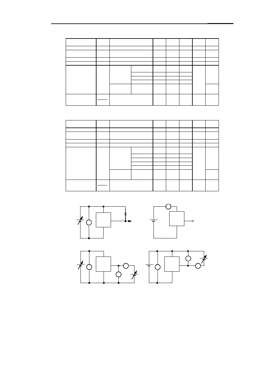
HIGH-PRECISION VOLTAGE DETECTOR
S-807 Series
Seiko Instruments Inc.
23
49. S-80763AN-JT-X (Detection voltage : 6.148 to 6.452 V)
(Unless otherwise specified : Ta=25
∞
C)
Parameter
Symbol
Conditions
Min.
Typ.
Max.
Unit
Test
circuit
Detection voltage
-V
DET
6.148
6.300
6.452
V
1
Hysteresis width
V
HYS
-V
DET
◊
0.02
-V
DET
◊
0.05
-V
DET
◊
0.08
V
1
Current consumption
I
SS
V
DD
= 7.5 V
1.9
3.6
µ
A
2
Operating voltage
V
DD
1.0
15.0
V
1
Output current
I
OUT
Nch
V
DS
= 0.5 V
V
DD
= 1.2 V
0.23
0.50
mA
3
V
DD
= 2.4 V
1.60
3.70
V
DD
= 3.6 V
3.18
7.00
V
DD
= 4.8 V
4.13
8.56
Pch (CMOS
output)
V
DS
= 0.5 V
V
DD
= 8.4 V
0.59
0.96
4
Temperature
characteristic of -
V
DET
Ta=-30
∞
C to 80
∞
C
±
0.81
mV/
∞
C
50. S-80777SN-J8-X (Detection voltage : 7.515 to 7.885 V)
(Unless otherwise specified : Ta=25
∞
C)
Parameter
Symbol
Conditions
Min.
Typ.
Max.
Unit
Test
circuit
Detection voltage
-V
DET
7.515
7.700
7.885
V
1
Hysteresis width
V
HYS
-V
DET
◊
0.02
-V
DET
◊
0.05
-V
DET
◊
0.08
V
1
Current consumption
I
SS
V
DD
= 9.0 V
2.2
4.0
µ
A
2
Operating voltage
V
DD
1.0
15.0
V
1
Output current
I
OUT
Nch
V
DS
= 0.5 V
V
DD
= 1.2 V
0.23
0.50
mA
3
V
DD
= 2.4 V
1.60
3.70
V
DD
= 3.6 V
3.18
7.00
V
DD
= 4.8 V
4.13
8.56
V
DD
= 6.0 V
4.73
9.60
Pch (CMOS
output)
V
DS
= 0.5 V
V
DD
= 9.6 V
0.65
1.05
4
Temperature
characteristic of -
V
DET
Ta=-30
∞
C to 80
∞
C
±
0.99
mV/
∞
C
Test Circuits
(2)
V
DS
V
DS
V
DD
V
DD
V
DD
V
DD
OUT
V
SS
CRT
R(100 k
)*
OUT
V
DD
* R is unnecessary for CMOS output products.
V
SS
OUT
A
V
DD
V
SS
V
DD
V
A
V
OUT
V
SS
V
DD
A
V
(1)
(3)
(4)
V
V
Figure 8
S-807
Series
S-807
Series
S-807
Series
S-807
Series
-V
DET
Ta
-V
DET
Ta
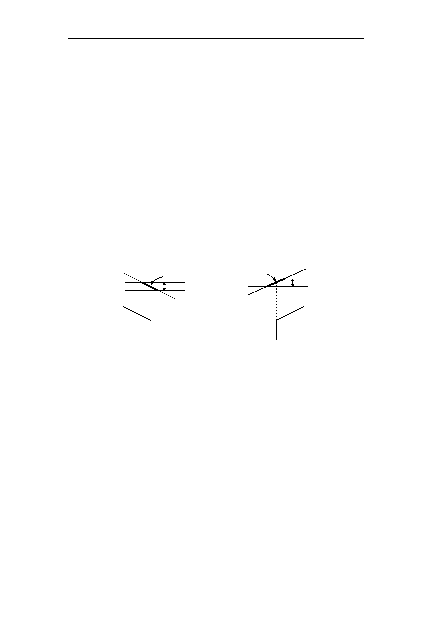
HIGH-PRECISION VOLTAGE DETECTOR
S-807 Series
24
Seiko Instruments Inc.
Technical Terms
1. Detection voltage (-V
DET
)
Detection voltage -V
DET
is the voltage at which the detector
'
s output goes active. In products with
"
Nch open-drain
"
and
"
CMOS active low output
"
configurations the output goes low on detection. It goes high in products with CMOS active high
output configurations. This detection voltage varies slightly among products of the same type. The variation of voltages
between the specified minimum [(-V
DET
)min.] and maximum [(-V
DET
)max.] values is called the detection voltage range. (See
Figure 9.)
Example : For the S-80745AN, detection voltage lies in the range
4.392
(-V
DET
)
4.608.
2. Release voltage (+V
DET
)
Release voltage +V
DET
is the voltage at which a unit
'
s output returns (is
"
released
"
) to its inactive state (high for Nch and
CMOS active low output configurations, and low for CMOS active high output configurations). The value of this voltage for
any single unit lies in a range determined from the value of that unit
'
s detection voltage (see Figure 10):
(-V
DET
)
◊
1.02
(+V
DET
)
(-V
DET
)
◊
1.08.
Example : For an S-80745AN with -V
DET
=4.608, release voltage lies in the range 4.700
(+V
DET
)
4.997.
For an S-80745AN with -V
DET
=4.392, release voltage lies in the range 4.480
(+V
DET
)
4.743.
When calculating the overall release voltage range for S-807 Series products, care must be taken to consider the variation in
the series
'
detection voltage values. The minimum and maximum values for release voltage [(+V
DET
)min. and (+V
DET
)max.)]
must be determined using (-V
DET
)min. and (-V
DET
)max.:
(+V
DET
)min.=[(-V
DET
)min.]
◊
1.02;
(+V
DET
)max.=[(-V
DET
)max.]
◊
1.08.
Example : For S-80745AN voltage detectors, release voltage lies in the range 4.480
(+V
DET
)
4.977.
Note :
Detection voltage(-V
DET
) and Release voltage(+V
DET
) range equally from 4.480V to 4.608V, however, (+V
DET
) >
(-V
DET
).
3. Hysteresis width (V
HYS
)
Hysteresis width is the voltage difference between a device
'
s detection voltage and its release voltage (see Figure 14.
V
HYS
=B-A). By giving a device hysteresis, erroneous toggling of the output due to noise at the input is avoided.
4. Through-type current
Through-type current refers to the instantaneous current flow which occurs at the moment a voltage detector output toggles.
This current is quite large in devices with CMOS configured outputs, and also occurs to some extent in Nch open-drain
configured devices. S-807 Series voltage detectors are specially designed to limit through-type currents and are superior to
S-805 Series devices in this respect. (See current consumption characteristics.)
Release voltage range
Detection voltage range
V
DD
OUT
(-V
DET
)max.
(-V
DET
)min.
Detection voltage
Figure 9
(+V
DET
)max.
(+V
DET
)min.
V
DD
Release voltage
OUT
Figure 10
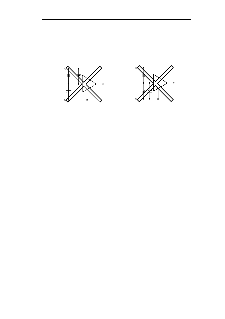
HIGH-PRECISION VOLTAGE DETECTOR
S-807 Series
Seiko Instruments Inc.
25
5. Oscillation
In applications where a resistor is connected to the voltage detector input (Figure 11 and 12), the through-type current
generated when the output goes from low to high (release) causes a voltage drop equal to [through-type current]
◊
[input
resistance] across the resistor. When the input voltage resultantly drops below the detection voltage -V
DET
, the output
voltage returns to its low level. In this state, the through-type current -- and its resultant voltage drop -- have disappeared,
and the output goes back from low to high. Again, a through-type current is generated, a voltage drop appears, and the
process repeats. Oscillation refers to this unstable condition
.
Figure 11
Figure 12
∑
Power reset mis-implementation
∑
Mis-implementation with input voltage
divider
Di
(CMOS output)
R
V
IN
V
SS
V
DD
C
OUT
S-
807XXAL
/SL
RB
RA
OUT
V
IN
V
SS
V
DD
(CMOS output)
S-
807XXAL
/SL
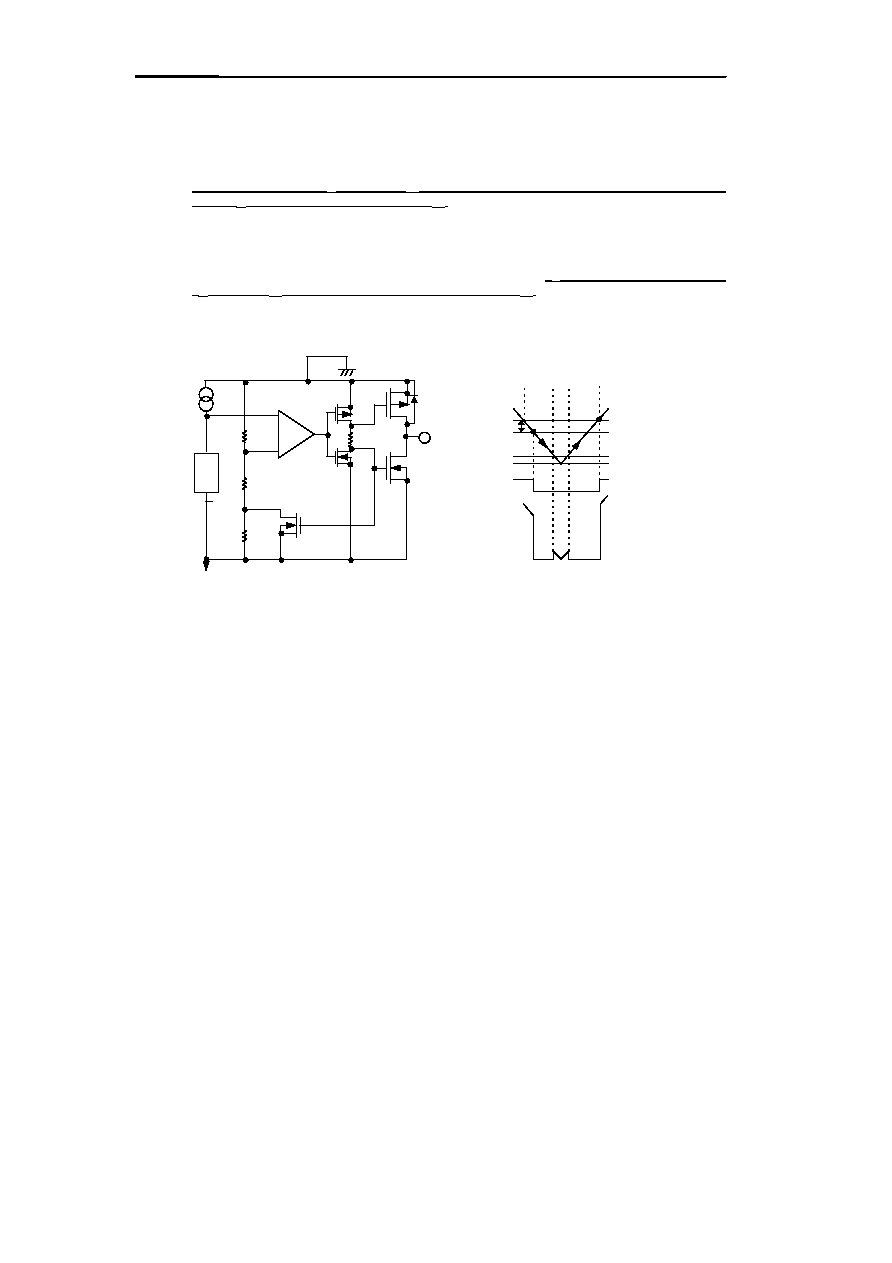
HIGH-PRECISION VOLTAGE DETECTOR
S-807 Series
26
Seiko Instruments Inc.
Operation
1. Basic operation
(1) When power supply voltage V
DD
is greater than the release voltage +V
DET
, the Nch transistor is OFF and the Pch
transistor ON, causing V
DD
(high) to appear at the output. With the Nch transistor of Figure 13 (a) off, the comparator
input voltage is (RB+RC)/(RA+RB+RC)
◊
V
DD
.
(2) When power supply voltage V
DD
goes below +V
DET
, the output continues to maintain the power supply voltage level, as
long as V
DD
remains above the detection voltage -V
DET
. When V
DD
does fall below -V
DET
(A in Figure 14), the Nch
transistor goes ON, the Pch transistor goes OFF, and V
SS
appears at the output. With the Nch transistor of Figure 13
(a) ON, the comparator input voltage is RB/(RA+RB)
◊
V
DD
.
(3) When V
DD
falls below the minimum operating voltage, the output becomes undefined. However, output will revert to V
DD
if a pull-up has been employed.
(4) V
SS
will again be output when V
DD
rises above the minimum operating voltage. V
SS
will continue to be output even when
V
DD
surpasses -V
DET
, as long as it does not exceed the release voltage +V
DET
.
(5) When V
DD
rises above +V
DET
(B in Figure 14), the Nch transistor goes OFF, the Pch transistor goes ON, and V
DD
appears at the output.
V
DD
RB
V
SS
V
REF
RC
RA
(a)
-
+
OUT
Pch
Nch
*
Hysteresis
width
(V
HYS
)
A
B
V
DD
V
SS
OUT
V
DD
V
SS
(1)
(2)
(3)
(5)
(4)
Figure 14
Figure 13
Minimum operating
voltage
Release voltage(+V
DET
)
Detection voltage(-V
DET
)
Comparator
output
* Parasitic diode
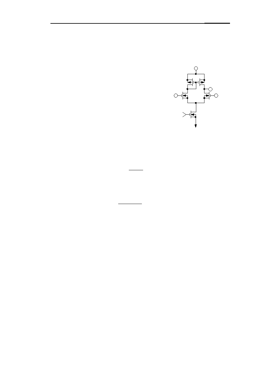
HIGH-PRECISION VOLTAGE DETECTOR
S-807 Series
Seiko Instruments Inc.
27
4. Other characteristics
(1) Temperature characteristic of detection voltage
Because of the excellent temperature characteristic of the reference voltage circuit, the temperature characteristics of
the detection voltage are expressed by the following formula in the range of -30
∞
C to +80
∞
C.
*-V
REF
is 0.65 V min., 0.8 V typ., 0.95 V max.
(2) Temperature characteristic of release voltage
V
IN
+
V
SS
V
DD
V
OUT
F
igure 15 Comparator
V
IN
-
Bias
3. Comparator
The comparator drives a differential amplifier with a current
consumption of only 0.5
µ
A as shown in Figure 15.
It features:
∑
Good matching characteristics
∑
Wide operating voltage range
∑
Low offset voltage
2. Reference voltage circuit
The S-807 Series has 0.8 V typical reference voltage circuit as-
V
REF
(a high-stable reference voltage source) .
It features:
∑
Low power consumption
∑
Good temperature characteristic
-V
REF
-V
REF
-V
DET
-V
DET
+V
HYS
◊
(
±
0.1) mV/
∞
C
typ.
◊
(
±
0.1) mV/
∞
C
HIGH-PRECISION VOLTAGE DETECTOR
S-807 Series
28
Seiko Instruments Inc.
Dimensions
(1) TO-92
(2) SOT-89-3
(3) SOT-23-5
Unit : mm
0.45
±
0.1
12.7 min.
1.5 max.
4.2 max.
0.8 max.
0.45
±
0.1
0.6 max.
5.2 max.
5.0
±
0.2
2.3 max.
1.27
±
0.05
1.27
±
0.05
0.95
±
0.1
2.8
0.4
±
0.1
0 min.
1.1
±
0.1
1.3 max.
1.6
2.9 (3.1 max.)
+0.2
-0.3
0.95
±
0.1
1.9
±
0.2
0.16
+0.1
-0.06
0.45
Mark side
Figure 16 Dimensions
0.8 min.
2.5
±
0.2
4.0
1.5
±
0.2
0.4
±
0.05
0.45
±
0.1
1.5
±
0.1
1.5
±
0.1
4.5
±
0.2
1.6
±
0.2
0.4
±
0.1
2.5
45
∞
(0.4)
(0.2)
+0.25
-0.35
(0.4)
0.4
±
0.1
1.5
±
0.1
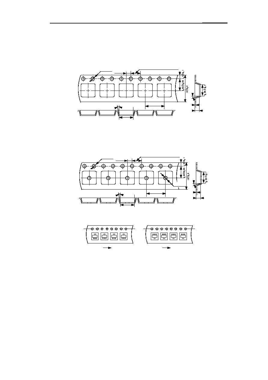
HIGH-PRECISION VOLTAGE DETECTOR
S-807 Series
Seiko Instruments Inc.
29
Taping
1. SOT-89-3
1.1 Tape specifications
T1 and T2 types are available depending upon the direction of ICs on the tape.
T2
T1
Unit : mm
Feed direction
Feed direction
(1) White label (without a hole in the center of embossed area)
(2) Blue label (with a hole in the center of embossed area)
3
∞
max.
2.0
±
0.05
1.5
4.0
±
0.1(10 pitches : 40.0
±
0.2)
4.75
±
0.1
8.0
±
0.1
+0.1
-0
0.3
±
0.05
2.0
±
0.1
5
∞
max.
3
∞
max.
2.0
±
0.05
1.5
4.0
±
0.1(10 pitches : 40.0
±
0.2)
4.75
±
0.1
8.0
±
0.1
+0.1
-0
0.3
±
0.05
2.0
±
0.1
5
∞
max.
1.5
+0.1
-0
Figure 17
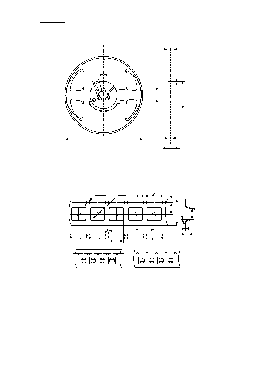
HIGH-PRECISION VOLTAGE DETECTOR
S-807 Series
30
Seiko Instruments Inc.
1.2 Reel specifications
1 reel holds 1000 detectors.
2. SOT-23-5
2.1 Tape specifications
T1 and T2 types are available depending upon the direction of ICs on the tape.
The top cover tape comes in two tones; opaque, transparent and transparent.
Figure 18
3
∞
max.
3.2
±
0.1
0.27
±
0.05
1.4
±
0.1
3
∞
max.
4.0
±
0.1
1.0
1.5
+0.1
-0
+0.2
-0
2.0
±
0.05
4.0
±
0.1(10 pitches : 40.0
±
0.2)
1.75
±
0.1
3.5
±
0.05
8.0
±
0.2
T2
T1
Unit : mm
Feed direction
Feed direction
Figure 19
180
+
0
-
3
16.5 Max.
60
+
1
0
Most outer dimension.
(1.5)
13.0
±
0.3
Inner dimension of reel core.
15.4
±
1.0
Outer dimension of reel core.
10.5
±
0.4
13
±
0.2
(60
∞
)
(60
∞
)
2
±
0.2
Unit : mm
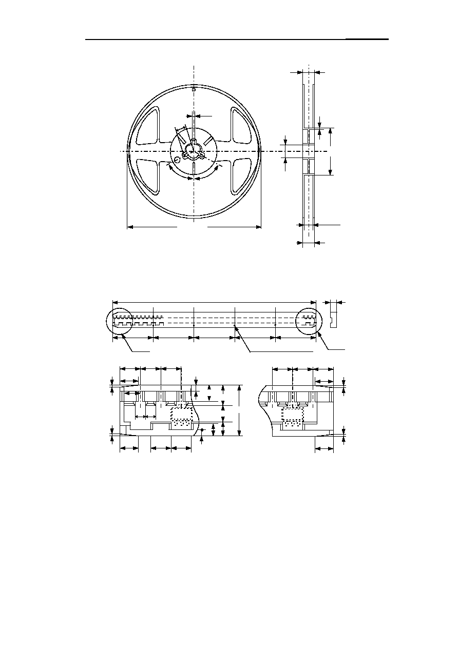
HIGH-PRECISION VOLTAGE DETECTOR
S-807 Series
Seiko Instruments Inc.
31
2.2. Reel specifications
1 reel holds 3000 detectors.
Magazine Dimensions
1
stick holds 25 detectors.
Part B
5
±
0.1
38.4
35
35
35
34.8
178.2
±
0.1
Counting mark (every five units)
2.5
2.8
3.35
±
0.07 3.5
±
0.07
3.5
±
0.07
Part A
1.9
1.6
2.8
3.15
3.85
±
0.07
2.8
0.5
2.8
3.35
±
0.07
3.5
±
0.07
3.5
±
0.07
1.45
±
0.1
Unit : mm
"Part A"magnified
0.5
0.5
0.5
"Part B"magnified
1.45
±
0.1
4.1
±
0.07
2.6
±
0.1
10.0
±
0.1
3.25
±
0.1
2.7
±
0.07
Figure 21
Figure 20
180
+
0
-
3
12.5 Max.
60
+
1
0
Most outer dimension.
(1.5)
9.0
±
0.3
Inner dimension of reel core.
11.4
±
1.0
Outer dimension of reel core.
10.5
±
0.4
13
±
0.2
(60
∞
)
(60
∞
)
2
±
0.2
Unit : mm
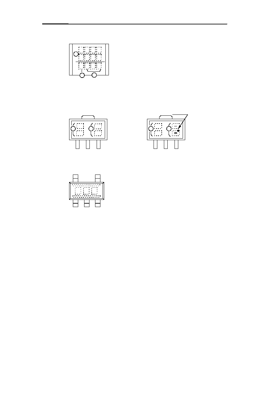
HIGH-PRECISION VOLTAGE DETECTOR
S-807 Series
32
Seiko Instruments Inc.
Markings
1
3
2
1
2
1. TO-92
4
0
A
N
S
8
0
7
9
A
1
1
2. SOT-89-3
(1) White label
1
2
3. SOT-23-5
(2) Blue label
Factory code
&
Product name (abbreviation)
&
Lot No.
: Alphabet
: Dot on one side
Product name
Last digit of the year
Lot No.
Product name (abbreviation)
Lot No.
Product name (abbreviation)
Lot No.
Figure 22
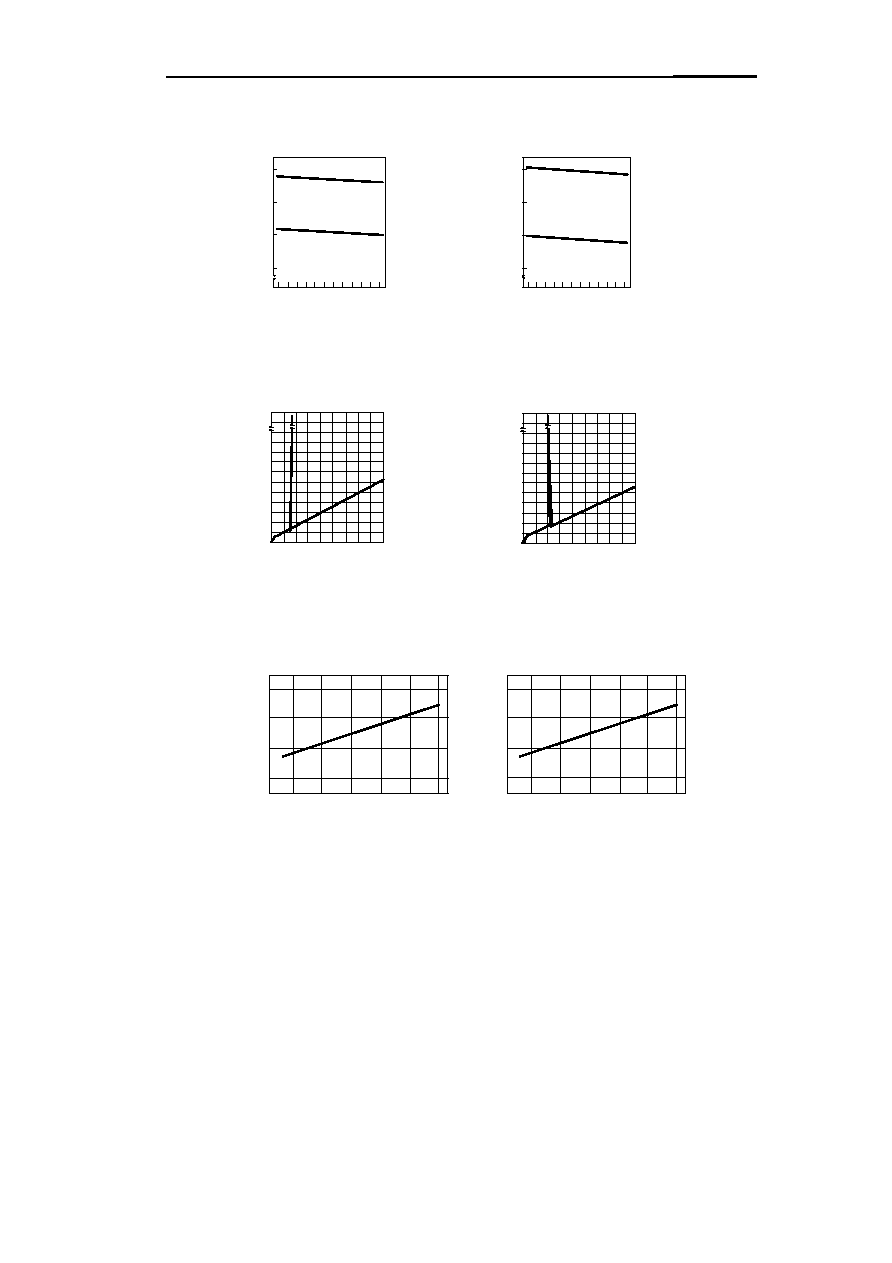
HIGH-PRECISION VOLTAGE DETECTOR
S-807 Series
Seiko Instruments Inc.
33
Characteristics
1. Detection voltage (V
DET
) - Temperature (Ta)
80
80
1.1 S-80730AL
1.2 S-80740AH
Release voltage
Detection voltage
3.2
3.1
3.0
2.9
V
DET
(V)
-20
0
20 40 60 80
Ta (
∞
C)
4.2
4.1
4.0
3.9
Release voltage
Detection voltage
V
DET
(V)
-20
0 20 40 60 80
Ta (
∞
C)
2. Current consumption (I
SS
) - Input voltage (V
IN
)
2.1 S-80730AL
2.2 S-80740AH
75.0
5.0
4.0
3.0
2.0
1.0
0
I
SS
(
µ
A)
2.0
6.0 10.0 14.0 18.0
140
5.0
4.0
3.0
2.0
1.0
0
I
SS
(
µ
A)
2.0
6.0 10.0 14.0 18.0
V
IN
(V)
V
IN
(V)
3. Current consumption (I
SS
) - Temperature (Ta)
3.1 S-80730AL
V
DD
=4.5 V
1.6
1.2
0.8
0.4
I
SS
(
µ
A)
-20
0
20
40
60
Ta (
∞
C )
3.2 S-80740AH
V
DD
=6.0 V
1.6
1.2
0.8
0.4
I
SS
(
µ
A)
-20
0
20
40
60
Ta (
∞
C )
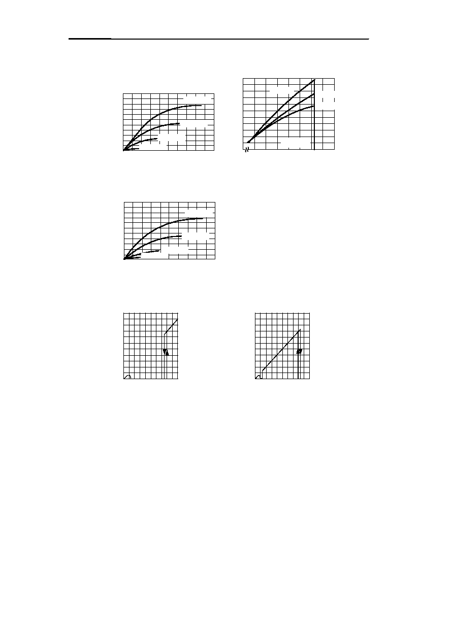
HIGH-PRECISION VOLTAGE DETECTOR
S-807 Series
34
Seiko Instruments Inc.
4. Output transistor current (I
OUT
)
4.1 Nch transistor current
V
DS
(V)
I
OUT
(mA)
V
DD
=4.8 V
V
DD
=3.6 V
V
DD
=2.4 V
V
DD
=1.2 V
40
32
24
16
8
0
1.0
2.0
3.0
4.0
5.0
(i) V
DS
-I
OUT
(ii) V
DD
-I
OUT
Ta=-30
∞
C
Ta=25
∞
C
Ta=80
∞
C
6.4
4.8
8.0
3.2
1.6
0
I
OUT
(mA)
1.2 1.6 2.0
2.4 2.8 3.2 3.6
4.0
V
DD
(V)
V
DS
=0.5 V
4.2 Pch transistor current
V
DS
-I
OUT
V
DD
=4.8 V
V
DD
=3.6 V
V
DD
=2.4 V
V
DD
=1.2 V
V
DS
(V)
1.0
2.0
3.0
4.0
5.0
I
OUT
(mA)
4.0
3.2
2.4
1.6
0.8
0
5.1 CMOS active low output
5.2 CMOS active high output
4.0
3.2
2.4
1.6
0.8
0
V
OUT
(V)
0.8 1.6 2.4 3.2 4.0
V
DD
(V)
5.0
4.0
3.0
2.0
1.0
0
V
OUT
(V)
1.0 2.0 3.0 4.0 5.0
V
DD
(V)
5. Minimum operating voltage
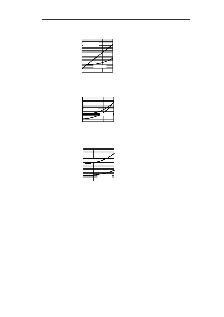
HIGH-PRECISION VOLTAGE DETECTOR
S-807 Series
Seiko Instruments Inc.
35
6. Dynamic response
6.1 Nch open-drain output products
6.2 CMOS active low output products
6.3 CMOS active high output products
RL=100 k
"L"
"H"
"H"
"L"
10
2
10
1
10
0
10
-1
Delay time
(ms)
10
-4
10
-3
10
-2
10
-1
Load capacitance (
µ
F)
"H"
"L"
10
-1
10
-2
10
-3
10
-4
10
-3
10
-2
10
-1
Load capacitance (
µ
F)
Delay time
(ms)
"L"
"H"
"H"
"L"
Delay time
(ms)
10
-4
10
-3
10
-2
10
-1
Load capacitance (
µ
F)
10
-1
10
-2
10
-3
10
-2
10
0
10
0
10
1
"L"
"H"
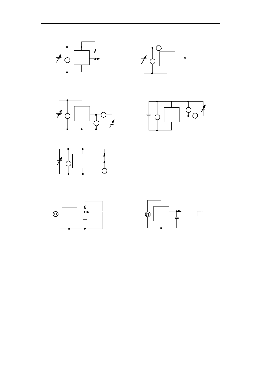
HIGH-PRECISION VOLTAGE DETECTOR
S-807 Series
36
Seiko Instruments Inc.
Measuring Circuits
OUT
Oscilloscope
V
DS
V
DD
V
DD
V
DD
(1) Detection voltage
V
SS
V
DD
V
S-807
Series
(2) Current consumption
A
V
SS
V
DD
V
S-807
Series
(3) Output transistor current
OUT
(b) Pch transistor current
(a) Nch transistor current
V
SS
V
DD
V
S-807
Series
A
V
V
DD
V
DS
V
SS
V
DD
V
S-807
Series
A
V
OUT
OUT
* R is unnecessary for CMOS output products.
*R(100 k
)
V
DD
(4) Min. operating voltage
V
OUT
V
SS
V
DD
S-807
(Nch output)
Series
V
(5) Dynamic response
(b) CMOS output products
(a) Nch open-drain output products
P.G
CRT
100 k
7 V
CL
V
SS
OUT
S-807
Series
V
DD
P.G
CRT
CL
V
SS
OUT
S-807
Series
V
DD
V
SS
1 V
5 V
Input pulse
*R (100 k
)
* R is unnecessary for CMOS output products.
Figure 23
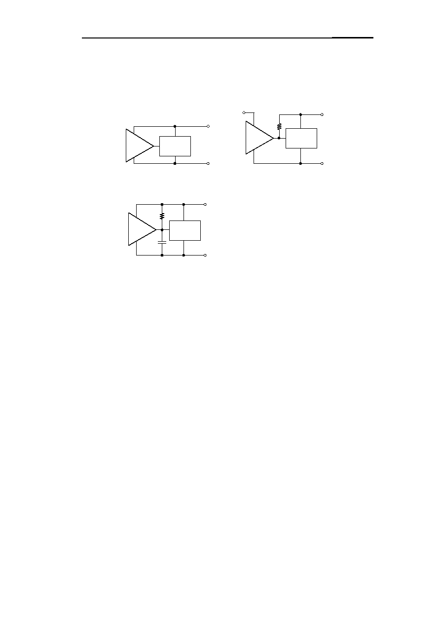
HIGH-PRECISION VOLTAGE DETECTOR
S-807 Series
Seiko Instruments Inc.
37
Application Circuit Examples
1. Reset circuits of microcomputers
If the power supply voltage to a microcomputer falls below the specified level, unspecified operation may be performed or the
contents of the memory register may be lost. When power supply voltage returns to normal, the microcomputer may need to
be initialized before normal operations can be done.
Reset circuits protect microcomputers, in the event of current being momentarily switched off or lowered.
With the S-807 Series, the reset circuits shown in Figures 24 to 26 can be easily constructed.
V
SS
V
DD
Micro-
computer
S-807XX
AL/SL
Figure 24
(Nch open-drain output products only)
V
DD1
V
SS
V
DD2
Figure 25
Micro-
computer
S-807XX
AN/SN
V
SS
V
DD
Micro-
computer
Figure 26
S-807XX
AN/SN
HIGH-PRECISION VOLTAGE DETECTOR
S-807 Series
38
Seiko Instruments Inc.
2. Power-on reset circuit
The Nch open-drain output products of the S-807 Series can be used to construct a power-on reset circuit. Following is an
example
.
Di
(Nch open-drain products)
R
OUT
V
IN
V
SS
V
DD
S-807XX
AN/SN
C
+
-
Figure 28
V
DD
(V)
t (s)
OUT
(V)
t (s)
Note 1: R should be 7.5k
or less for purpose of protection against oscillation.
Note 2:
"
Di
"
momentarily discharges the charge received via
"
C
"
at the falling edge of power off. There
is no need to insert a diode, when there is no conflict with application circuit even if there is a
delay in the falling edge of OUT at the falling edge of power off.
Note 3: When there is a sharp rise in power, the output voltage may go
"
H
"
momentarily in unstable range of
the output voltage (the output voltage is unstable below the minimum operating voltage) .
V
DD
(V)
t (s)
OUT
(V)
t (s)
Figure 27
(R
7.5k
)
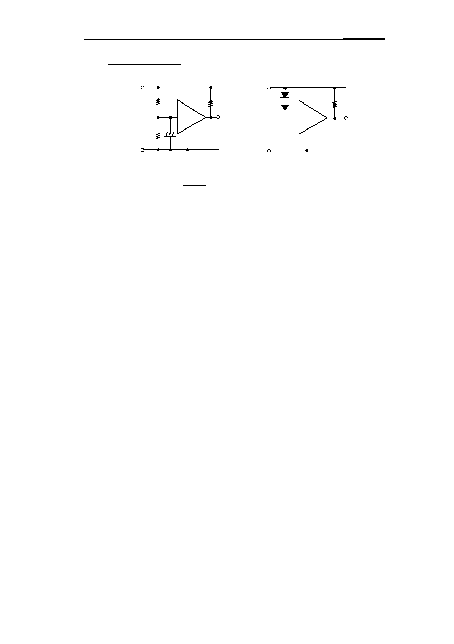
HIGH-PRECISION VOLTAGE DETECTOR
S-807 Series
Seiko Instruments Inc.
39
3. Change of detection voltage
In Nch open-drain output products of the S-807 Series, detection voltage can be changed with resistance dividers or diodes
as shown in Figures 29 and 30. In Figure 29, hysteresis width is also changed.
Notes
∑
In CMOS output products of S-807 Series, high through current flows when detecting or releasing. If a high impedance is
connected to the input, oscillation may be caused by the through current when lowering the voltage during releasing.
∑
In TO-92 products, since there are projections and resin burrs on the roots of the lead terminals formed at the Tiebar-cut, do
not solder to them.
∑
When designing for mass production using an application circuit described here, take into account the deviation of
components and temperature characteristics.
∑
Seiko Instruments Inc. cannot take any responsibility for the patents on the circuits described here.
Detection voltage=V
f1
+V
f2
+-V
DET
Figure 30
Figure 29
RB
RA
OUT
V
IN
V
S
V
DD
S-
807XX
AN/SN
+
-
(Nch open-drain
products)
(RA
7.5k
)
V
f2
V
f1
OUT
V
IN
V
SS
V
DD
S-
807XX
AN/SN
(Nch open-drain
products)
Figure 29
Detection voltage=
Hysteresis width=
∑
-V
DET
RA+RB
RB
∑
-V
HYS
RA+RB
RB
Note 1: The
hysteresis width will be a little
wider than the value of the formula
above, because of the through current,
if RA and RB are larger.
Note 2: RA should be 7.5k
or less for
purpose of protection against
oscillation.
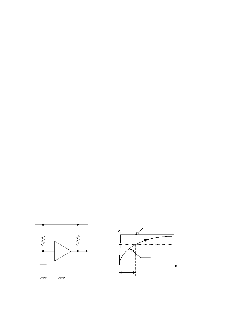
40
Collection of Product FAQs
Author: Hamaguchi Masanao
Date: 98/11/12 (Thursday) 10:17 (Modified: 98/12/14 (Monday) 16:42)
<Information level>
A:
Public (Printing O.K.)
Index:
B: Technical
<Product>
Division name: 01 IC
Category 1:
11 Power Supply
Category 2:
1. Voltage Detectors
Cal No.:
S-807
Related Documents:
Question:
What is the method for calculating delay-time of the power-on clear circuit?
Answer:
The delay time (power-on clear time) produced in a power-on clear circuit using the S-807xxAN can be
found by substituting constants in the following formula:
)
Vdd
+
Vdet
-
1
(
Ln
◊
R
◊
C
◊
1
=
Tdelay
Tdelay: Delay time [sec]
C: External capacitance value [F]
R: Resistance value [
]
V det+: S-807xxAN Series release voltage [V]
Vdd: Supply voltage [V]
V
S-807xxAN
Pull-up resistor
R
C
Vdd
S-807xxAN release voltage (Vdet+)
Delay time
S-807 input voltage
Supply voltage (Vdd)
Note: Set R to less than 7.5 k
to prevent oscillation.

41
<Remarks>
FAQ No.: 11S807001